ATA2516

Features: • Supply Voltage: 4.5 V to 5.5 V• Automatic Sensitivity Adaptation (AGC)• Automatic Strong Signal Adaptation (ATC)• Carrier Frequency is 56 kHz; Adjusted by Zener Diode Fusing ±4%• TTL and CMOS CompatibleSpecifications Parameters Symbol Value U...

product image

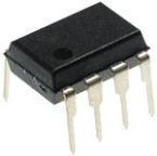
ATA2516 Picture
SeekIC No. : 004291072 Detail

ATA2516: Features: • Supply Voltage: 4.5 V to 5.5 V• Automatic Sensitivity Adaptation (AGC)• Automatic Strong Signal Adaptation (ATC)• Carrier Frequency is 56 kHz; Adjusted by Zener D...

floor Price/Ceiling Price

Part Number:
ATA2516
Supply Ability:
5000

Price Break

  • Qty
  • 1~5000
  • Unit Price
  • Negotiable
  • Processing time
  • 15 Days
Total Cost: $ 0.00

SeekIC Buyer Protection PLUS - newly updated for 2013!

  • Escrow Protection.
  • Guaranteed refunds.
  • Secure payments.
  • Learn more >>

Month Sales

268 Transactions

Rating

evaluate  (4.8 stars)

Upload time: 2024/12/24

Payment Methods

All payment methods are secure and covered by SeekIC Buyer Protection PLUS.

Notice: When you place an order, your payment is made to SeekIC and not to your seller. SeekIC only pays the seller after confirming you have received your order. We will also never share your payment details with your seller.
Product Details

Description


Features:

• Supply Voltage: 4.5 V to 5.5 V
• Automatic Sensitivity Adaptation (AGC)
• Automatic Strong Signal Adaptation (ATC)
• Carrier Frequency is 56 kHz; Adjusted by Zener Diode Fusing ±4%
• TTL and CMOS Compatible


Specifications

Parameters
Symbol
Value
Unit
Supply voltage
VS
-0.3 to 6
V
Supply current (DC current IIN_DC = 0)
IS
0.5
mA
Input voltage
VIN
-0.3 to VS
V
Input DC current at VS = 5 V
IIN_DC
0.8
mA
Output voltage
VO
-0.3 to VS
V
Operating temperature
Tamb
-40 to +85
°C
Storage temperature
Tstg
-40 to +125
°C
Power dissipation at Tamb = 25°C
Ptot
10
mW


Description

The IC ATA2516 is a complete IR receiver for data communication systems. The device is developed and optimized for use in carrier frequency modulated transmission applications. Its function can be described using the block diagram in Figure 1 on page 2. The input stage meets two main functions. First, it provides a suitable bias voltage for the PIN diode. Secondly, the pulsed photo current signals are transformed into a voltage by a special circuit which is optimized for low noise application. After amplification by a Controlled Gain Amplifier (CGA), the signals pass a tuned integrated narrow bandpass filter with a center frequency f0 equivalent to the chosen carrier frequency of the input signal. The demodulator is used to convert the input burst signal to a digital envelope output pulse and to evaluate the signal information quality, i.e., unwanted pulses will be suppressed at the output pin. All this is done by means of an integrated dynamic feedback circuit which varies the gain as a function of changing environmental conditions (ambient light, modulated lamps etc.). A 7-bit digital- to-analog converter is used to adjust the gain of the controlled gain amplifier. Other special features serve to adapt to the current application to secure best transmission quality. The ATA2516 operates in a voltage supply range of 4.5 V - 5.5 V.


Customers Who Bought This Item Also Bought

Margin,quality,low-cost products with low minimum orders. Secure your online payments with SeekIC Buyer Protection.
Boxes, Enclosures, Racks
Batteries, Chargers, Holders
Potentiometers, Variable Resistors
Motors, Solenoids, Driver Boards/Modules
Isolators
Sensors, Transducers
View more