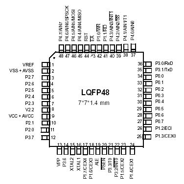
Features: • 80C51 Compatible
Five I/O Ports
Two 16-bit Timer/Counters
256 Bytes RAM
• 8K Bytes ROM/OTP Program Memory with 64 Bytes Encryption Array and 3 Security Levels
• High-Speed Architecture
33 MHz at 5V (66 MHz Equivalent)
X2 Speed Improvement Capability (6 Clocks/Machine Cycle)
• 10-bit, 8 Channels A/D Converter
• Hardware Watchdog Timer with Reset-out
• Programmable I/O Mode: Standard C51, Input Only, Push-pull, Open Drain
• Asynchronous Port Reset
• Full Duplex Enhanced UART with Baud Rate Generator
• SPI, Master Mode
• Dual System Clock
Crystal or Ceramic Oscillator (33/40 MHz)
Internal RC Oscillator (12 MHz)
Programmable Prescaler
• Programmable Counter Array with High-speed Output, Compare/Capture, Pulse Width Modulation and Watchdog Timer Capabilities
• Interrupt Structure
8 Interrupt Sources
4 Interrupt Priority Levels
• Power Control Modes
Idle Mode
Power-down Mode
Power-off Flag
• Power Supply: 2.7 - 5.5V
• Temperature Range: Industrial (-40 To 85°C)
• Package: LQFP48 (Body 7*7*1.4 mm), PLCC52
ApplicationSoftware can take advantage of the additional data pointers to both increase speed and reduce code size, for example, block operations (copy, compare, search...) are well served by using one data pointer as a 'source' pointer and the other one as a "destination" pointer.
ASSEMBLY LANGUAGE
; Block move using dual data pointers
; Destroys DPTR0, DPTR1, A and PSW
; note: DPS exits opposite of entry state
; unless an extra INC AUXR1 is added
;
00A2 AUXR1 EQU 0A2H
;
0000 909000MOV DPTR,#SOURCE ; address of SOURCE
0003 05A2 INC AUXR1 ; switch data pointers
0005 90A000 MOV DPTR,#DEST ; address of DEST
0008 LOOP:
0008 05A2 INC AUXR1 ; switch data pointers
000A E0 MOVX A,atDPTR ; get a byte from SOURCE
000B A3 INC DPTR ; increment SOURCE address
000C 05A2 INC AUXR1 ; switch data pointers
000E F0 MOVX atDPTR,A ; write the byte to DEST
000F A3 INC DPTR ; increment DEST address
0010 70F6JNZ LOOP ; check for 0 terminator
0012 05A2 INC AUXR1 ; (optional) restore DPS
INC is a short (2 bytes) and fast (12 clocks) way to manipulate the DPS bit in the AUXR1 SFR. However, note that the INC instruction does not directly force the DPS bit to a particular state, but simply toggles it. In simple routines, such as the block move example, only the fact that DPS is toggled in the proper sequence matters, not its actual value. In other words, the block move routine works the same whether DPS is '0' or '1' on entry. Observe that without the last instruction (INC AUXR1), the routine will exit with DPS in the opposite state.Pinout Specifications
C = commercial.................................................... 0°C to 70°C
I = industrial .................................................... -40°C to 85°C
Storage Temperature ................................. -65°C to + 150°C
Voltage on VCC to VSS ...........................................-0.5V to + 7V
Voltage on VPP to VSS .........................................-0.5V to + 13V
Voltage on Any Pin to VSS.............................-0.5V to VCC + 0.5V
Power Dissipation................................................................. 1 W |
DescriptionThe AT8xC5112 is a high performance ROM/OTP version of the 80C51 8-bit microcontroller.
The AT8xC5112 retains all the features of the standard 80C51 with 8 Kbytes ROM/OTP program memory, 256 bytes of internal RAM, a 8-source, 4-level interrupt system, an on-chip oscillator and two timer/counters.
The AT8xC5112 is dedicated for analog interfacing applications. For this, it has a 10-bit, 8 channels A/D converter and a five channels Programmable Counter Array.
In addition, the AT8xC5112 has a Hardware Watchdog Timer, a versatile serial channel that facilitates multipro-cessor communication (EUART) with an independent baud rate generator, a SPI serial bus controller and a X2 speed improvement mechanism.
The X2 feature allows to keep the same CPU power at a divided by two oscillator frequency.
The fully static design of the AT8xC5112 allows to reduce system power consumption by bringing the clock frequen-cy down to any value, even DC, without loss of data.
The AT8xC5112 has 3 software-selectable modes of reduced activity for further reduction in power consumption. In the idle mode, the CPU is frozen while the peripherals are still operating. In the quiet mode, the A/D converter is only operating. In the Power-down mode, the RAM is saved and all other functions are inoperative. Two oscillators source, crystal and RC, provide a versatile power management.
The AT8xC5112 is proposed in 48-/52-pin count packages with Port 0 and Port 2 (address/data buses).

 AT83C5112 Data Sheet


