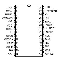
Features: • Smart Card Interface
Compliance with ISO 7816, EMV2000, GIE-CB, GSM and WHQL Standards Card Clock Stop High or Low for Card Power-down Modes Support Synchronous Cards with C4 and C8 Contacts Card Detection and Automatic de-activation Sequence Programmable Activation Sequence
Direct Connection to the Smart Card
Logic Level Shifters
Short Circuit Current Limitation (see electrical characteristics)
8kV+ ESD Protection (MIL/STD 883 Class 3)
Programmable Voltage
5V ±5% at 65 mA (Class A)
3V ±0.2V at 65 mA (Class B)
1.8V ±0.14V at 40 mA
Low Ripple Noise: < 200 mV
• Versatile Host Interface
ICAM (Conditional Access) Compatible
Two Wire Interface (TWI) Link
Programmable Address Allow up to 8 Devices
Programmable Interrupt Output
Automatic Level Shifter (1.6V to VCC)
• Reset Output Includes
Power-On Reset (POR)
Power-Fail Detector (PFD)
• High-efficiency Step-up Converter: 80 to 98% Efficiency
• Extended Voltage Operation: 3V to 5.5V
• Low Power Consumption
180 mA Maximum In-rush Current
30 µA Typical Power-down Current (without Smart Card)
• 4 to 48 MHz Clock Input, 7 MHz Min for Step-up Converter (for AT83C24)
• 18 to 48MHz Clock input (for AT83C24NDS)
• Industrial Temperature Range: -40 to +85°C
• Packages: SO28 and QFN28
Pinout Specifications
|
Ambient Temperature Under Bias: ...................-40°C to 85°C
Storage Temperature: ................................ -65°C to +150°C
Voltage on VCC: .......................................... VSS -0.5V to +6.0V
Voltage on SCIB pins (***): ............CVSS -0.5V to CVCC + 0.5V
Voltage on host interface pins:..........VSS -0.5V to EVCC + 0.5V
Voltage on other pins: ....................... VSS -0.5V to VCC + 0.5V
Power Dissipation: ........................................................... 1.5W
Thermal resistor of QFN package..(**).........................35°C/W
Thermal resistor of SO package.....................................48°C/W
|
DescriptionThe AT83C24 is a smart card reader interface IC for smart card reader/writer applications such as EFT/POS terminals and set top boxes. It enables the management of any type of smart card from any kind of host. Up to 8 AT83C24 can be connected in parallel using the programmable TWI address.
Its high efficiency DC/DC converter, low quiescent current in standby mode makes it particularly suited to low power and portable applications. The reduced bill of material allows reducing significantly the system cost. A sophisticated protection system guarantees timely and controlled shutdown upon error conditions.
The AT83C24NDS is a dedicated version approved by NDS for use with NDS Video- Guard conditional access software in set-top boxes. All AT83C24 datasheet is applicable to AT83C24NDS. The main differences between AT83C24 and AT83C24NDS are listed below:
1/ CLASS A card supplied with CVCC = 4.75 to 5.25V for AT83C24NDS,
CLASS A card supplied with CVCC = 4.6 to 5.25V for AT83C24
2/ 18MHz minimum on input clock for AT83C24NDS
3/ Up to 10µF for capacitor connected on CVCC pin for AT83C24,
3.3µF mandatory for AT83C24NDS

 AT83C24 Data Sheet


