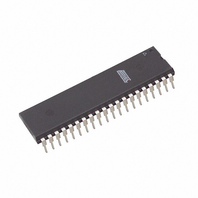
DescriptionThe AT80251G2D is designed as 8/16-bit microcontroller with serial communication interfaces. It is tailored to 8/16-bit microcontroller applications requiring an increased instruction throughput, a reduced operating frequency or a larger addressable memory space. The architecture can pr...
AT80251G2D: DescriptionThe AT80251G2D is designed as 8/16-bit microcontroller with serial communication interfaces. It is tailored to 8/16-bit microcontroller applications requiring an increased instruction thr...
SeekIC Buyer Protection PLUS - newly updated for 2013!
268 Transactions
All payment methods are secure and covered by SeekIC Buyer Protection PLUS.
The AT80251G2D is designed as 8/16-bit microcontroller with serial communication interfaces. It is tailored to 8/16-bit microcontroller applications requiring an increased instruction throughput, a reduced operating frequency or a larger addressable memory space. The architecture can provide a significant code size reduction when compiling C programs while fully preserving the legacy of C51 assembly routines.
AT80251G2D has many features and some are lised here. (1)Pin and software compatibility with standard 80C51 products and 80C51Fx /Rx /Rx+. (2)Plug-in replacement of intel's 8xC251Sx. (3)C251 core: intel's MCS 251 D-step compliance. (4)40-byte register file. (5)Registers accessible as bytes, words or dwords. (6)Three-stage instruction pipeline. (7)16-bit internal code fetch. (8)Enriched C51 instruction set. (9)16-bit and 32-bit ALU. (10)Compare and conditional jump instructions. (11)Expanded set of move instructions. (12)Linear addressing. (13)1 Kbyte of on-chip RAM. (14)External memory space (code /data) programmable from 64 kilobytes to 256 kilobytes. (15)Power-on reset (integrated on the chip). (16)Power-off flag (cold and warm resets). (17)Software programmable system clock. And so on.
Some AT80251G2D absolute maximum ratings have been concluded into several points as follow. (1)Its storage temperature range would be from -65°C to +150°C. (2)Its voltage on any other pin to Vss would be from -0.5V to +6.5V. (3)Its Iol per IO pin would be 15mA. (4)Its power dissipation would be 1.5W. (5)Its ambient temerature under bias would be from 0°C to 70°C for commercial and would be from -40°C to +85°C for industrial and would be from -40°C to +85°C for automotive. It should be noted that stresses above those listed in absolute maximum ratings may cause permanent damage to device.
Also some AT80251G2D DC characteristics are concluded as follow. (1)Its input low voltage (SCL,SDA) would be min -0.5V and max 0.3Vdd. (2)Its input high voltage (RST, SCL, SDA) would be min 0.7Vdd and max Vdd+0.5V. (3)Its Vdd data retention limit would be max 1.8V. And so on. If you have any question or suggestion or want to know more information please contact us for details. Thank you!