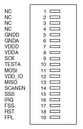
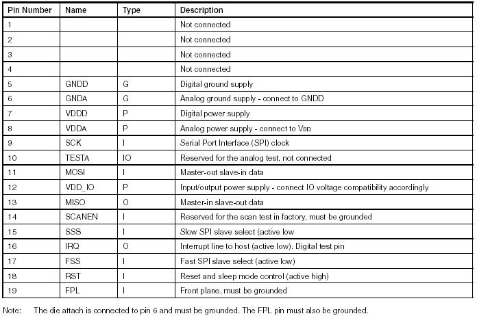
Features: •Thermal Sensitive Layer Over a 0.35 µm CMOS Array•Image Zone: 0.4 x 11.6 mm•Image Array: 8 * 232 = 1856 Pixels•Pixel Pitch: 50 * 50 µm = 500 dpi Resolution•On-chip 8-bit Analog to Digital Converter•Serial Peripheral Interface (SPI) - 2 Mod...
AT77C105A: Features: •Thermal Sensitive Layer Over a 0.35 µm CMOS Array•Image Zone: 0.4 x 11.6 mm•Image Array: 8 * 232 = 1856 Pixels•Pixel Pitch: 50 * 50 µm = 500 dpi Resolu...
SeekIC Buyer Protection PLUS - newly updated for 2013!
268 Transactions
All payment methods are secure and covered by SeekIC Buyer Protection PLUS.
Parameter |
Symbol |
Comments |
Value |
Note: Stresses beyond those listed under "Absolute Maximum Ratings" may cause permanent damage to the device. These are stress ratings only and functional operation of the device at these or any other conditions beyond those indicated in the operational sections of this specification is not implied. Exposure to absolute maximum rating conditions for extended periods may affect device reliability. |
Power supply voltage |
VDDD,VDDA |
0.5 to 4.6V | ||
Front plane |
FPL |
GND to VDD +0.5V | ||
Digital input |
SSS, FSS,SCK,MOSI |
GND to VDD +0.5V | ||
Input/output pads power supply |
VDD_IO |
GND to VDD +0.5V | ||
Storage temperature |
Tstg |
-50 to +95°C | ||
Lead temperature (soldering 10 seconds) |
Tleads |
Do not solder |
Forbidden |