Features: • 1.65V - 1.95V Read/Write
• High Performance
Random Access Time 70 ns
Page Mode Read Time 20 ns
Synchronous Burst Frequency 66 MHz
Configurable Burst Operation
• Sector Erase Architecture
Sixteen 4K Word Sectors with Individual Write Lockout
Two Hundred Fifty-four 32K Word Main Sectors with Individual Write Lockout
• Typical Sector Erase Time: 32K Word Sectors 500 ms; 4K Word Sectors 100 ms
• Thirty-two Plane Organization, Permitting Concurrent Read in Any of the Thirty-one Planes not Being Programmed/Erased
• Suspend/Resume Feature for Erase and Program
Supports Reading and Programming Data from Any Sector by Suspending Erase of a Different Sector
Supports Reading Any Word by Suspending Programming of Any Other Word
• Low-power Operation
30 mA Active
10 A Standby
• VPP Pin for Write Protection and Accelerated Program/Erase Operations
• RESET Input for Device Initialization
• CBGA and TSOP Packages
• Seventeen 128-bit Protection Registers (2,176 Bits)
• Common Flash Interface (CFI)Pinout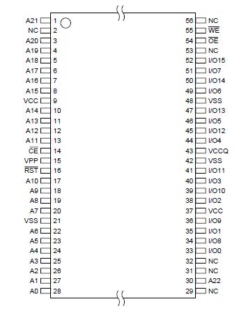 SpecificationsTemperature under Bias ................................ -55°C to +125°C
Storage Temperature ..................................... -65°C to +150°C
All Input Voltages Except VPP
(including NC Pins)
with Respect to Ground ...................................-0.6V to +6.25V
VPP Input Voltage
with Respect to Ground ......................................... 0V to 12.5V
All Output Voltages
with Respect to Ground ...........................-0.6V to VCCQ + 0.6V
*NOTICE: Stresses beyond those listed under "Absolute Maximum Ratings" may cause permanent damage to the device. This is a stress rating only and functional operation of the device at these or any other conditions beyond those indicated in the operational sections of this specification is not implied. Exposure to absolute maximum rating conditions for extended periods may affect device reliability.DescriptionThe AT49SN/SV12804 is a 1.8-volt 128-megabit Flash memory. The memory is divided into multiple sectors and planes for erase operations. The AT49SN/SV12804 is organized as 8,388,608 x 16 bits. The device can be read or reprogrammed off a single 1.8V power supply, making it ideally suited for In-System programming. The device can be configured to operate in the asynchronous/page read (default mode) or burst read mode (not available for the AT49SV12804). The burst read mode is used to achieve a faster data rate than is possible in the asynchronous/page read mode. If the
AVD and the CLK signals are both tied to GND and the burst configuration register is configured to perform asynchronous reads, the device will behave like a standard asynchronous Flash memory. In the page mode, the
AVD signal can be tied to GND or can be pulsed low to latch the page address. In both cases the CLK can be tied to GND.
The AT49SN/AT49SV12804 is divided into thirty-two memory planes. A read operation can occur in any of the thirty-one planes which is not being programmed or erased. This concurrent operation allows improved system performance by not requiring the system to wait for a program or erase operation to complete before a read is performed. To further increase the flexibility of the device, it contains an Erase Suspend and Program Suspend feature. This feature will put the erase or program on hold for any amount of time and let the user read data from or program data to any of the remaining sectors. There is no reason to suspend the erase or program operation if the data to be read is in another memory plane.
The AT49SV12804 VPP pin provides data protection and faster programming and erase times. When the V
PP input is below 0.4V, the program and erase functions are inhibited. When V
PP is at 0.9V or above, normal program and erase operations can be performed. With V
PP at 12.0V, the program (Dual-word Program command) and erase operations are accelerated.

 AT49SV12804 Data Sheet