Features: ` Low Voltage Operation
- 2.7V Read
- 5V Program/Erase
` Fast Read Access Time - 120 ns
` Internal Erase/Program Control
` Sector Architecture
- One 8K Words (16K bytes) Boot Block with Programming Lockout
- Two 8K Words (16K bytes) Parameter Blocks
- One 232K Words (464K bytes) Main Memory Array Block
` Fast Sector Erase Time - 10 seconds
` Word-By-Word Programming - 10 s/Word
` Hardware Data Protection
` DATA Polling For End Of Program Detection
` Low Power Dissipation
- 25 mA Active Current
- 50 A CMOS Standby Current
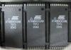
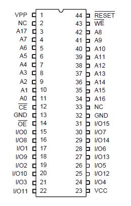
` Typical 10,000 Write CyclesPinout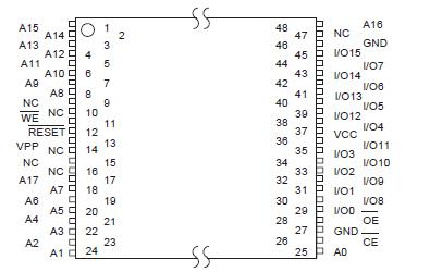
 SpecificationsTemperature Under Bias................. -55°C to +125°C
Storage Temperature...................... -65°C to +150°C
All Input Voltages
(including NC Pins)
with Respect to Ground ................... -0.6V to +6.25V
All Output Voltages
with Respect to Ground .............-0.6V to VCC + 0.6V
Voltage on OE
with Respect to Ground ................... -0.6V to +13.5V
*NOTICE: Stresses beyond those listed under "Absolute Maximum Ratings" may cause permanent damage to the device. This is a stress rating only and functional operation of the device at these or any other conditions beyond those indicated in the operational sections of this specification is not implied. Exposure to absolute maximum rating conditions for extended periods may affect device reliability. DescriptionThe AT49BV4096 and AT49LV4096 are 3-volt, 4-megabit Flash Memories organized as 256K words of 16 bits each. Manufactured with Atmel's advanced nonvolatile CMOS technology, the devices offer access times to 120 ns with power dissipation of just 67 mW at 2.7V read. When deselected, the CMOS standby current is less than 50 A.
To allow for simple in-system reprogrammability, the AT49BV4096/AT49LV4096 does not require high input voltages for programming. Reading data out of the device is similar to reading from an EPROM; it has standard
CE,
OE, and
WE inputs to avoid bus contention. Reprogramming the AT49BV4096/LV4096 is performed by first erasing a block of data and then programming on a word-by-word basis.
The device AT49LV4096 is erased by executing the erase command sequence; the device internally controls the erase operation. The memory is divided into three blocks for erase operations. There are two 8K word parameter block sections and one sector consisting of the boot block and the main memory array block. The AT49BV4096/LV4096 is programmed on a word-by-word basis.
The device AT49LV4096 has the capability to protect the data in the boot block; this feature is enabled by a command sequence. Once the boot block programming lockout feature is enabled, the data in the boot block cannot be changed when input levels of 3.6 volts or less are used. The typical number of program and erase cycles is in excess of 10,000 cycles.
The optional 8K word boot block section AT49LV4096 includes a reprogramming lock out feature to provide data integrity. The boot sector is designed to contain user secure code, and when the feature is enabled, the boot sector is protected from being reprogrammed.During a chip erase, sector erase, or word programming, the VPP pin must be at 5V ± 10%.

 AT49LV4096 Data Sheet