AT49LH00B4

Features: • Complies with Intel® Low-Pin Count (LPC) Interface Specification Revision 1.1 Supports both Firmware Hub (FWH) and LPC Memory Read and Write Cycles• Auto-detection of FWH and LPC Memory Cycles Can Be Used as FWH for Intel 8xx, E7xxx, and E8xxx Series Chipsets Can Be ...

product image

AT49LH00B4 Picture
SeekIC No. : 004290401 Detail

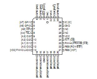
AT49LH00B4: Features: • Complies with Intel® Low-Pin Count (LPC) Interface Specification Revision 1.1 Supports both Firmware Hub (FWH) and LPC Memory Read and Write Cycles• Auto-detection of FW...

floor Price/Ceiling Price

Part Number:
AT49LH00B4
Supply Ability:
5000

Price Break

  • Qty
  • 1~5000
  • Unit Price
  • Negotiable
  • Processing time
  • 15 Days
Total Cost: $ 0.00

SeekIC Buyer Protection PLUS - newly updated for 2013!

  • Escrow Protection.
  • Guaranteed refunds.
  • Secure payments.
  • Learn more >>

Month Sales

268 Transactions

Rating

evaluate  (4.8 stars)

Upload time: 2024/9/16

Payment Methods

All payment methods are secure and covered by SeekIC Buyer Protection PLUS.

Notice: When you place an order, your payment is made to SeekIC and not to your seller. SeekIC only pays the seller after confirming you have received your order. We will also never share your payment details with your seller.
Product Details

Description


Features:

• Complies with Intel® Low-Pin Count (LPC) Interface Specification Revision 1.1
   Supports both Firmware Hub (FWH) and LPC Memory Read and Write Cycles
• Auto-detection of FWH and LPC Memory Cycles
   Can Be Used as FWH for Intel 8xx, E7xxx, and E8xxx Series Chipsets
   Can Be Used as LPC Flash for Non-Intel Chipsets
• Top Boot with Bottom Partitioned Memory Array for Efficient Vital Data Storage
    64-Kbyte Top Boot Sector, Six 64-Kbyte Sectors, One 32-Kbyte Sector,
   One 16-Kbyte Sector, Two 8-Kbyte Sectors
   Or Memory Array Can Be Divided Into Eight Uniform 64-Kbyte Sectors for Erasing
• Two Configurable Interfaces
   FWH/LPC Interface for In-System Operation
   Address/Address Multiplexed (A/A Mux) Interface for Programming during Manufacturing
• FWH/LPC Interface
   Operates with the 33 MHz PCI Bus Clock
   5-signal Communication Interface Supporting Byte Reads and Writes
   Two Hardware Write Protect Pins: TBL for Top Boot Sector and WP for All Other Sectors
   Five General-purpose Input (GPI) Pins for System Design Flexibility
   Identification (ID) Pins for Multiple Device Selection
   Sector Locking Registers for Individual Sector Read and Write Protection
• A/A Mux Interface
   11-pin Multiplexed Address and 8-pin Data Interface
   Facilitates Fast In-System or Out-of-System Programming
• Single Voltage Operation
   3.0V to 3.6V Supply Voltage for Read and Write Operations
• Industry-Standard Package Options
   32-lead PLCC
   40-lead TSOP


Pinout

  Connection Diagram


Specifications

Voltage on Any Pin ...................-0.5V to +VCC + 0.5V(1)(2)


Description

The AT49LH00B4 is a Flash memory device designed for use in PC and notebook BIOS applications. The device complies with version 1.1 of Intel's LPC Interface Spec-ification, providing support for both FWH and LPC memory read and write cycles. The device can also automatically detect the memory cycle type to allow the AT49LH 00B4 to be used as a FWH with Intel chipsets or as an LPC Flash with non-Intel chipsets.


Customers Who Bought This Item Also Bought

Margin,quality,low-cost products with low minimum orders. Secure your online payments with SeekIC Buyer Protection.
Motors, Solenoids, Driver Boards/Modules
Memory Cards, Modules
Prototyping Products
DE1
Computers, Office - Components, Accessories
Cable Assemblies
View more