Features: • 3.0V to 3.6V Read/Write• Burst Read Performance <100 MHz (RAS Latency = 2, CAS Latency = 6), 10 ns Cycle Time tSAC = 7 ns <75 MHz (RAS Latency = 2, CAS Latency = 5), 13 ns Cycle Time tSAC = 8 ns <50 MHz (RAS Latency = 1, CAS Latency = 4), 20 ns Cycle Time tSAC = 9 ...
AT49LD3200: Features: • 3.0V to 3.6V Read/Write• Burst Read Performance <100 MHz (RAS Latency = 2, CAS Latency = 6), 10 ns Cycle Time tSAC = 7 ns <75 MHz (RAS Latency = 2, CAS Latency = 5), 13...
SeekIC Buyer Protection PLUS - newly updated for 2013!
268 Transactions
All payment methods are secure and covered by SeekIC Buyer Protection PLUS.
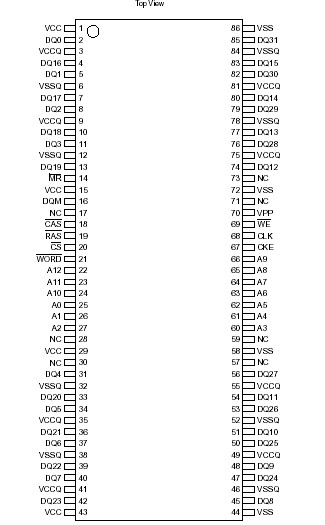
The AT49LD3200 or AT49LD3200B SFlash™ is a synchronous, high-bandwidth Flash memory fabricated with Atmel's high-performance CMOS process technology and is organized either as 2,097,152 x 16 bits (word mode) or as 1,048,576 x 32 bits (double word mode), depending on the polarity of the WORD pin (see Pin Function Description Table). Synchronous design allows precise cycle control. I/O transactions are possible on every clock cycle. All operations are synchronized to the rising edge of the system clock. The range of operating frequencies, programmable burst length and programmable latencies allow the same device to be useful for a variety of high-bandwidth, high-performance memory system applications.
The AT49LD3200B will automatically activate the Asynchronous Boot Block after power-up, whereas with the AT49LD3200, the Asynchronous Boot Block can be activated through Mode Register Set.
The synchronous DRAM interface AT49LD3200 allows designers to maximize system performance while eliminating the need to shadow slow asynchronous Flash memory into highspeed RAM.The 32-megabit SFlash device is designed to sit on the synchronous memory bus and operate alongside SDRAM.