Features: Single Voltage Operation
5V Read
5V Programming
Fast Read Access Time - 55 ns
Internal Erase/Program Control
Sector Architecture
One 8K Words (16K bytes) Boot Block with Programming Lockout
Two 4K Words (8K bytes) Parameter Blocks
One 240K Words (480K bytes) Main Memory Array Block
Fast Sector Erase Time - 10 seconds
Byte-by-Byte or Word-By-Word Programming - 10 µs Typical
Hardware Data Protection
DATA Polling For End Of Program Detection
Low-Power Dissipation
50 mA Active Current
300 µA CMOS Standby Current
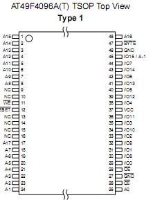
Typical 10,000 Write CyclesPinout SpecificationsTemperature Under Bias.............................-55°C to +125°C
Storage Temperature..................................-65°C to +150°C
All Input Voltages
(including NC Pins)
with Respect to Ground...................................-0.6V to +6.25V
All Output Voltages
with Respect to Ground.............................-0.6V to VCC+ 0.6V
Voltage on RESET
with Respect to Ground...................................-0.6V to +13.5VDescriptionThe AT49F004(T) and AT49F4096A(T) are 5-volt, 4-megabit Flash Memories orga-nized as 524,288 words of 8 bits each or 256K words of 16 bits each. Manufactured with Atmel's advanced nonvolatile CMOS technology, AT49F4096AT offer access times to 55 ns with power dissipation of just 275 mW. When deselected, the CMOS standby current is less than 300 µA.
AT49F4096AT contains a user-enabled "boot block" protection feature. Two versions of the feature are available: the AT49F004/4096A locates the boot block at lowest order
addresses ("bottom boot"); the AT49F004T/4096AT locates AT49F4096AT at highest order addresses ("top boot").
To allow for simple in-system reprogrammability, the AT49F004(T)/4096A(T) does not require high input voltages for programming. Reading data out of AT49F4096AT is similar to reading from an EPROM; it has standard CE, OE, and WE
inputs to avoid bus con-tention. Reprogramming the AT49F004(T)/4096A(T) is performed by first erasing a(continued)

 AT49F4096AT Data Sheet


