Features: • Single 2.7V - 3.6V Supply
• Dual-interface Architecture
Dedicated Serial Interface (SPI Modes 0 and 3 Compatible)
Dedicated Parallel I/O Interface (Optional Use)
• Page Program Operation
Single Cycle Reprogram (Erase and Program)
8192 Pages (1056 Bytes/Page) Main Memory
• Supports Page and Block Erase Operations
• Two 1056-byte SRAM Data Buffers Allows Receiving of Data while Reprogramming the Flash Array
• Continuous Read Capability through Entire Array
Ideal for Code Shadowing Applications
• Low-power Dissipation
4 mA Active Read Current Typical
2 µA CMOS Standby Current Typical
• 20 MHz Maximum Clock Frequency Serial Interface
• 5 MHz Maximum Clock Frequency Parallel Interface
• Hardware Data Protection
• Commercial and Industrial Temperature Ranges
Pinout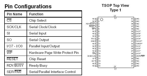 Description
The AT45DB642 is a 2.7-volt only, dual-interface Flash memory ideally suited for a wide variety of digital voice-, image-, program code- and data-storage applications. The dualinterface of the AT45DB642 allows a dedicated serial interface to be connected to a DSP and a dedicated parallel interface to be connected to a microcontroller or vice versa.
However, the use of either interface is purely optional. Its 69,206,016 bits of memory are organized as 8192 pages of 1056 bytes each. In addition to the main memory, the AT45DB642 also contains two SRAM data buffers of 1056 bytes each. The buffers allow receiving of data while a page in the main memory is being reprogrammed, as well as reading or writing a continuous data stream. EEPROM emulation (bit or byte alterability) is easily handled with a selfcontained three step Read-Modify-Write operation. Unlike conventional Flash memories that are accessed randomly with multiple address lines and a parallel interface, the DataFlash
® uses either a serial interface or a parallel interface to sequentially access its data. The simple sequential access facilitates hardware layout, increases system reliability, minimizes switching noise, and reduces package size and active pin count. DataFlash supports SPI mode 0 and mode 3. AT45DB642 is optimized for use in many commercial and industrial applications where high-density, low-pin count, low-voltage, and low-power are essential. AT45DB642 operates at clock freque-ncies up to 20 MHz with a typical active read current consumption of 4 mA.
To allow for simple in-system reprogrammability, the AT45DB642 does not require high input voltages for program-ming. The device operates from a single power supply, 2.7V to 3.6V, for both the program and read operations. The AT45DB642 is enabled through the chip select pin (CS) and accessed via a three-wire interface consisting of the Serial Input (SI), Serial Output (SO), and the Serial Clock (SCK), or a parallel interface consisting of the parallel input/output pins (I/O7 - I/O0) and the clock pin (CLK). The SCK and CLK pins are shared and provide the same clocking input to the DataFlash.
All programming cycles of AT45DB642 are self-timed, and no separate erase cycle is required before programming.
When AT45DB642 is shipped from Atmel, the most significant page of the memory array may not be erased. In other words, the contents of the last page may not be filled with FFH.

 AT45DB642 Data Sheet


