Features: • Single 2.7V - 3.6V Supply
• Sequential Access, Parallel I/O Architecture
• Page Program Operation
Single Cycle Reprogram (Erase and Program)
4096 Pages (264 Bytes/Page) Main Memory
• Two 264-Byte Data Buffers Allows Receiving of Data while Reprogramming of Non-Volatile Memory
• Internal Program and Control Timer
• Fast Page Program Time 7 ms Typical
• 120 ms Typical Page to Buffer Transfer Time
• Low Power Dissipation
4 mA Active Read Current Typical
2 mA CMOS Standby Current Typical
• 2 MHz Max Clock Frequency
• Hardware Data Protection Feature
• Synchronous Clocking (Two Modes)
• CMOS and TTL Compatible Inputs and Outputs
• Commercial and Industrial Temperature Ranges
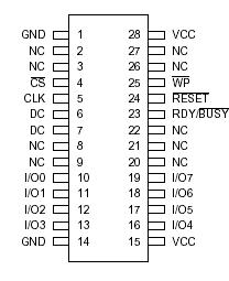
Pinout
 Specifications
|
Temperature under Bias .................... -55°C to +125°C
Storage Temperature ........................ -65°C to +150°C
All Input Voltages
(including NC Pins)
with Respect to Ground .........................-0.6V to +6.25V
All Output Voltages
with Respect to Ground ....................-0.6V to VCC + 0.6V
|
DescriptionThe AT45DB080 is a 2.7-volt only, sequential access, parallel interface Flash memory suitable for in-system repro-gramming. Its 8,650,752 bits of memory are organized as 4096 pages of 264-bytes each. In addition to the main memory, the AT45DB080 also contains two data buffers of 264-bytes each. The buffers allow receiving of data while a page in the main memory is being reprogrammed. Unlike conventional Flash memories that are accessed randomly with multiple address lines and a parallel interface, the DataFlash uses a parallel interface to sequentially access AT45DB080 data. The simple sequential access facilitates hardware layout, increases system reliability, minimizes switching noise, and reduces package size and active pin count. AT45DB080 is optimized for use in many commercial and industrial applications where high density, low pin count, low voltage, and low power are essential. Typical applications for the DataFlash are digital voice storage, image storage, and data storage. AT45DB080 operates at clock frequencies up to 2 MHz with a typical active read current consumption of 4 mA.
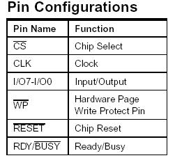
To allow for simple in-system reprogrammability, the AT45DB080 does not require high input voltages for program-ming. The device operates from a single power supply, 2.7V to 3.6V, for both the program and read operations. The AT45DB080 is enabled through the chip select pin (CS ) and accessed via an interface consisting of the parallel input/output (I/O7-I/O0) pins and the clock (CLK) pin. All programming cycles are self-timed, and no separate erase cycle is required before programming.

 AT45DB080 Data Sheet


