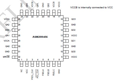
Features: · Configurable 10 outputs LVCMOS Clock distribution buffer· Compatible to single, dual and mixed 3.3V/2.5V Voltage supply· Wide range output clock frequency up to 250MHz· Designed for mid-range to high-performance telecom, networking and computer a...
ASM2I99456: Features: · Configurable 10 outputs LVCMOS Clock distribution buffer· Compatible to single, dual and mixed 3.3V/2.5V Voltage supply· Wide range output clock frequency u...
SeekIC Buyer Protection PLUS - newly updated for 2013!
268 Transactions
All payment methods are secure and covered by SeekIC Buyer Protection PLUS.
Symbol |
Characteristics |
Min |
Max |
Unit |
VCC |
Supply Voltage |
-0.3 |
4.6 |
V |
VIN |
DC Input Voltage |
-0.3 |
VCC+0.3 |
V |
VOUT |
DC Output Voltage |
-0.3 |
VCC+0.3 |
V |
IIN |
DC Input Current |
±20 |
mA | |
IOUT |
DC Output Current |
±50 |
mA | |
TS |
Storage temperature |
-40 |
125 |
°C |
The ASM2I99456 is a 2.5V and 3.3V compatible 1:10 clock distribution buffer designed for low-Voltage mid-range to high-performance telecom, networking and computing applications. Both 3.3V, 2.5V and dual supply voltages are supported for mixed-voltage applications. The ASM2I99456 offers 10 low-skew outputs and a differential LVPECL clock input. The outputs are configurable and support 1:1 and 1:2 output to input frequency ratios. The ASM2I99456 is specified for the extended temperature range of 40 to 85°C.
The ASM2I99456 is a full static design supporting clock frequencies up to 250 MHz. The signals are generated and retimed on-chip to ensure minimal skew between the three output banks.
Each of the three output banks can be individually supplied by 2.5V or 3.3V supporting mixed voltage applications. The FSELx ASM2I99456 pins choose between division of the input reference frequency by one or two. The frequency divider can be set individually for each of the three output banks. The ASM2I99456 can be reset and the outputs are disabled by deasserting the MR/OE pin (logic high state). Asserting MR/OE will enable the outputs.
All control inputs of ASM2I99456 accept LVCMOS signals while the outputs provide LVCMOS compatible levels with the capability to drive terminated 50 transmission lines. The clock input is low voltage PECL compatible for differential clock distribution support. Please consult the ASM2I99446 specification for a full CMOS compatible device. For series terminated transmission lines, each of the ASM2I99456 outputs can drive one or two traces giving the devices an effective fanout of 1:20. The device is packaged in a 7x7 mm2 32-lead LQFP and TQFP Packages.