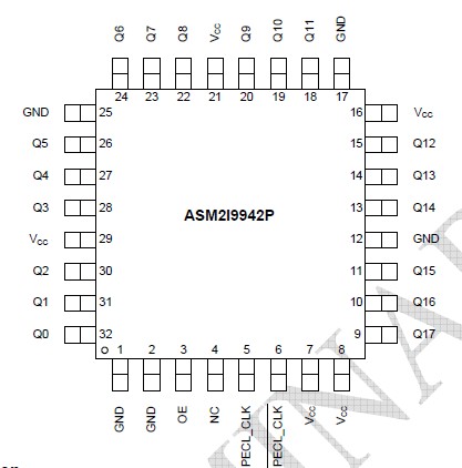
Features: `LVPECL Clock Input`2.5V LVCMOS Outputs for Pentium IITM* Microprocessor Support`200pS Maximum Targeted OutputtoOutput Skew`Maximum Output Frequency of 250MHz @3.3 VCC`32Lead LQFP and TQFP Packaging`Single 3.3V or 2.5V Supply`Pin and Function compatible with MPC942PPinoutSpecifications ...
ASM2I9942P: Features: `LVPECL Clock Input`2.5V LVCMOS Outputs for Pentium IITM* Microprocessor Support`200pS Maximum Targeted OutputtoOutput Skew`Maximum Output Frequency of 250MHz @3.3 VCC`32Lead LQFP and TQFP...
SeekIC Buyer Protection PLUS - newly updated for 2013!
268 Transactions
All payment methods are secure and covered by SeekIC Buyer Protection PLUS.
Symbol |
Parameter |
Min |
Max |
Unit |
VCC | Supply Voltage |
-0.3 |
3.6 |
V |
VI | Input Voltage |
-0.3 |
VCC + 0.3 |
V |
IIN | nput Current |
±20 |
mA | |
TStor | Storage Temperature Range |
-40 |
125 |
The ASM2I9942P is a 1:18 low voltage clock distribution chip with 2.5V or 3.3V LVCMOS output capabilities. The device is offered in two versions; the ASM2I9942C has an LVCMOS input clock while the ASM2I9942P has a LVPECL input clock. The 18 outputs are 2.5V or 3.3V LVCMOS compatible and feature the drive strength to drive 50 series or parallel terminated transmission lines. With output-to-output skews of 200pS, the ASM2I9942P is ideal as a clock distribution chip for the most demanding of synchronous systems. The 2.5V outputs also make the device ideal for supplying clocks for a high performance Pentium IITM microprocessor based design. With low output impedance (12), in both the HIGH and LOW logic states, the output buffers of the ASM2I9942P are ideal for driving series terminated transmission lines.
With an output impedance of 12, the ASM2I9942P can drive two series terminated transmission lines from each ouput. This capability gives the ASM2I9942P an effective fanout of 1:36. The ASM2I9942P provides enough copies of low skew clocks for most high performance synchronous systems.
The differential LVPECL inputs of the ASM2I9942P allow the device to interface directly with a LVPECL fanout buffer to build very wide clock fanout trees or to couple to a high frequency clock source. The OE pins will place the outputs into a high impedance state. The OE pin has an internal pullup resistor.
The ASM2I9942P is a single supply device. The VCC power pins require either 2.5V or 3.3V. The 32 lead LQFP and TQFP package is chosen to optimize performance, board space and cost of the device. The 32lead LQFP and TQFP have a 7x7mm2 body size with conservative 0.8mm pin spacing.