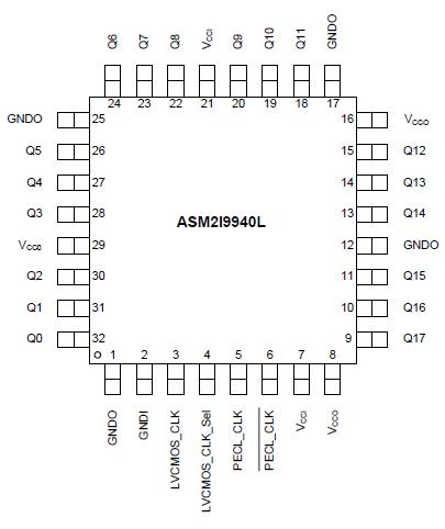
Features: ·LVPECL or LVCMOS Clock Input·2.5V LVCMOS Outputs for Pentium II Microprocessor Support*·150pS Maximum Output-to-Output Skew·Maximum Output Frequency of 250MHz·32 Lead LQFP & TQFP Packaging·Dual or Single Supply Device:·Dual VCC Supply Voltage, 3.3V Core and 2.5V Output·Single 3.3V V...
ASM2I9940L: Features: ·LVPECL or LVCMOS Clock Input·2.5V LVCMOS Outputs for Pentium II Microprocessor Support*·150pS Maximum Output-to-Output Skew·Maximum Output Frequency of 250MHz·32 Lead LQFP & TQFP Pack...
SeekIC Buyer Protection PLUS - newly updated for 2013!
268 Transactions
All payment methods are secure and covered by SeekIC Buyer Protection PLUS.
Symbol |
Parameter |
Min |
Max |
Unit |
VCC |
Supply Voltage |
-0.3 |
3.6 |
V |
VI |
Input Voltage |
-0.3 |
Vcc+0.3 |
V |
IIN |
Input Current |
±20 |
mA | |
Ttor |
Storage Temperature Range |
-40 |
125 |
|
Ts |
Max. Soldering Temperature (10 sec) |
260 |
||
TDV |
Static Discharge Voltage (As per JEDEC STD22- A114-B) |
2 |
kv |
The ASM2I9940L is a 1:18 low Voltage Clock distribution chip with 2.5V or 3.3V LVCMOS output capabilities. The device features the capability to select either a differential LVPECL or LVCMOS compatible input. The 18 outputs are 2.5V or 3.3V LVCMOS compatible and feature the drive strength to drive 50 series or parallel terminated transmission lines. With output-to-output skews of 150pS, the ASM2I9940L is ideal as a clock distribution chip for the most demanding of Synchronous systems. The 2.5V outputs also make the device ideal for supplying clocks for a high performance microprocessor based design. With low output impedance (20), in both the HIGH and LOW logic states, the output buffers of the ASM2I9940L are ideal for driving series terminated transmission lines.
With a 20 output impedance the ASM2I9940L has the capability of driving two series terminated lines from each output. This gives the device an effective fanout of 1:36.The differential LVPECL inputs of the ASM2I9940L allow the device to interface directly with a LVPECL fanout buffer to build very wide clock fanout trees or to couple to a high frequency clock source. The LVCMOS input provides a more standard interface for applications requiring only a single clock distribution chip at relatively low frequencies. In addition, the two clock sources can be used to provide for a test clock interface as well as the primary system clock. A logic HIGH on the LVCMOS_CLK_Sel pin will select the LVCMOS level clock input. All inputs of the ASM2I9940L have internal pullup/pulldown resistor, so they can be left open if unused.
The ASM2I9940L is a single or dual supply device. The device power supply offers a high degree of flexibility. The device can operate with a 3.3V core and 3.3V output, a 3.3V core and 2.5V outputs as well as a 2.5V core and 2.5V outputs. The 32-lead LQFP and TQFP Packages were chosen to optimize performance, board space and cost of ASM2I9940L. The 32-lead LQFP and TQFP Packages have a 7x7mm2 body size with conservative 0.8mm pin spacing.