Features:
Multipurpose control ASIC for OMNIFET (SGS Thompson intelligent power FET family)
Contains one channel on-chip
Applicable in low or high side switch circuits
Supply voltage range 10V 60V
Up to +/- 3V potential difference between system's digital ground and power ground possi-ble.
Current controlled interface
Provides load circuit surveillance and fault back signal
Typical rise time shorter then 2.4us
Typical fall time shorter then 3.8us
8 pin SOIC Package
Pinout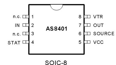 Specifications
| SYMBOL |
PARAMETER |
MIN |
MAX |
NOTE |
| VTR - VPGND |
DC Supply Voltage |
-0.5 V |
55 V |
|
| VDL |
Load Dump Voltage |
|
60V |
DIN 40839 vol. 2: 5 pulse, 500ms with
Ri = 2 Ohm |
| IINmax |
Maximum Input Cur-
rent |
-30 mA |
30 mA |
VIN < VInmin respectively VIN > VTR |
| VINA |
Digital input level |
VPGND -0.3V |
55V |
|
| Tstrg |
Storage Temperature |
-55 |
150 |
|
| Tsold |
Soldering Temperature |
|
260 |
1) |
| tsold |
Soldering Time |
|
10 sec |
Reflow and Wave |
| H |
Humidity |
5 % |
85 % |
|
| ESD |
Electrostatic Discharge |
1000 V |
|
HBM: R = 1.5 k, C = 100 pF |
DescriptionThe ASIC's purpose is to drive one OMNIFET n-channel power FET device. (OMNIFET is a trademark of SGS-THOMSON). The OMNIFET'sAS8401 integrated protection circuits (current limita-tion, over temperature protection, ...) are supplied via the OMNIFET's gate input. Thus in the OMNIFET's on-state, a DC gate current of 0.5mA is required. In a failure case (e.g. excessive
temperature) an internal resistor of about 100W is connected between the OMNIFET's gate and source. This state is used to detect errors by the controlling ASIC.
The control ASIC's standard application is in the use as a high side or low side switch (select-able) in a 24V-supply system, where the functionality of AS8401 is guaranteed up to a maximum driver
voltage of 55V.
In the load dump case (VTR = 60V, Pulse duration about 5ms, 5 pulses) the ASIC remains functioning (function state A) with modified parameters AS8401 (rise times and fall times).
The ASIC AS8401 contains one driver circuit (OMNIFET driver) and realises the following functions:
Current controlled on switch / off switch with defined rise, fall and delay times (programma-ble externally at the control input), that is usable as a high side or low side switch.
Automatic mode change between low side and high side use. This allows processing both,relatively low driver voltages (up to 25V, low side switch) and high driver voltages (up to 60V, high side switch) by detecting the present driver voltage related to OMNIFET's source potential.
Error detection for the OMNIFET and generation of an error status signal.
Gate to source voltage limitation for the OMNIFET to a maximum of 13V (OMNIFET pro-tection).
Floating ground interface between the controlling processor (control and status signal) and the driven OMNIFET; provided by separation of digital and power ground. The OMNIFET's source potential is the ASIC's ground.
Power reduction in the off-state (Supply current falling to less than 80A after switching the ASIC off).
The driver can be used as low or high side switch.
The control and the fault back signal are realised with current sources in order to guarantee the separation of digital ground (of the processor) and power ground (at the load circuit). This
is a safety function for a broken ASIC ground line and it fulfils EMC demands.
In applications as a high side driver the OMNIFET's source is connected to the ASIC ground,which switches together with the load circuit. Changes in the ASIC's ground potential of up to 58V, and rise and fall speeds of up to 58V/s are permitted.

 AS8401 Data Sheet


