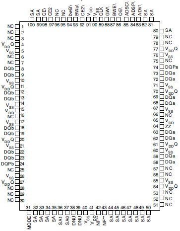
Features: • Fast access times: 8, 10, and 15ns• Fast clock speed: 113, 100, and 66 MHz• Fast clock and OE\ access times• Single +3.3V +0.3V/-0.165V power supply (VDD)• SNOOZE MODE for reduced-power standby• Common data inputs and data outputs• Individual B...
AS5SS256K18: Features: • Fast access times: 8, 10, and 15ns• Fast clock speed: 113, 100, and 66 MHz• Fast clock and OE\ access times• Single +3.3V +0.3V/-0.165V power supply (VDD)• ...
SeekIC Buyer Protection PLUS - newly updated for 2013!
268 Transactions
All payment methods are secure and covered by SeekIC Buyer Protection PLUS.
The Austin Semiconductor, Inc. Synchronous Burst SRAM family employs high-speed, low power CMOS designs that are fabricated using an advanced CMOS process.
ASI's 4Mb Synchronous Burst SRAMs integrate a 256K x 18, SRAM core with advanced synchronous peripheral circuitry and a 2-bit burst counter. All synchronous inputs pass through registers controlled by a positive-edge-triggered single clock input (CLK). The synchronous inputs include all addresses, all data inputs, active LOW chip enable (CE\), two additional chip enables for easy depth expansion (CE2\, CE2), burst control inputs (ADSC\, ADSP\, ADV\), byte write enables (BWx\) and global write (GW\).
Asynchronous inputs of AS5SS256K18 include the output enable (OE\), clock (CLK) and snooze enable (ZZ). There is also a burst mode input (MODE) that selects between interleaved and linear burst modes. The data-out (Q) of AS5SS256K18 , enabled by OE\, is also asynchronous. WRITE cycles can be from one to two bytes wide, as controlled by the write control inputs. Burst operation can be initiated with either address status processor (ADSP\) or address status controller (ADSC\) inputs. Subsequent burst addresses of AS5SS256K18 can be internally generated as controlled by the burst advance input (ADV\).
Address and write control are registered on-chip to simplify WRITE cycles. AS5SS256K18 allows self-timed WRITE cycles. Individual byte enables allow individual bytes to be written. During WRITE cycles on this x18 device BWa\ controls DQa pins and DQPa; BWb\ controls DQb pins and DQPb. GW\ LOW causes all bytes to be written. Parity bits are available on this device.
ASI's 4Mb Synchronous Burst SRAMs operate from a +3.3V VDD power supply, and all inputs and outputs are TTL-compatible. AS5SS256K18 is ideally suited for 486, Pentium®, and PowerPC systems and those systems that benefit from a wide synchronous data bus.