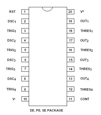
Features: • High speed operation -- 2MHz typical oscillation at 5V
• Each discharge output sinking current: 40mA at 5V
• Guaranteed low operating supply voltage of 2 to 12V
• Each timer is functionally equivalent to NE555 with greatly expanded high and low frequency ranges
• High speed, low power, monolithic CMOS technology
• Low supply current 150mA typical
• Extremely low trigger, threshold and reset currents -- 10pA typical
• Operates in both monostable and astable modes
• Fixed 50% duty cycle or adjustable duty cycle
• CMOS, NMOS and TTL compatible input/output
• Low supply current spikesApplication• High speed one-shot (monostable) pulse generation
• Precision timing
• Sequential timing
• Long delay timer
• Pulse width and pulse position modulation
• Missing pulse detector
• Frequency divider
• Synchronized timerPinout SpecificationsSupply voltage, V+ 13.2V
Input voltage range -0.3V to V+ +0.3V
Power dissipation 600 mW
Operating temperature range PE, SE package 0°C to + 70°C
DE package -55°C to +125°C
Storage temperature range -65°C to +150°C
Lead temperature, 10 seconds +260°CDescriptionThe ALD4501 timer is a high performance QUAD monolithic timing circuit built with advanced silicon gate CMOS technology. ALD4501 offers the benefits of high input impedance, thereby allowing smaller timing capacitors and longer timing cycle; high speed with typical cycle time of 500ns; low power dissipation for battery operated environment; and reduced supply current spikes allowing smaller and lower cost decoupling capacitors. Each of the four timers can be independently operated in either the monostable, astable, or 50% duty cycle mode.
Each ALD4501 timer is capable of producing accurate time delays and oscillations in both monostable and astable operation. ALD4501 operates in the one-shot (monostable) mode or 50% duty cycle free running oscillation mode with a single resistor and one capacitor. The inputs and outputs are fully compatible with CMOS, NMOS or TTL logic.
There are three matched internal resistors (approximately 200KW each) that set the threshold and trigger levels at two-thirds and one-third respectively
of V+. These levels can be adjusted by using the control terminal. When the trigger input is below the trigger level, the output is in the high state and sourcing 2mA. When the threshold input is above the threshold level at the same time the trigger input is above the trigger level, the internal flip-flop is reset, the output goes to the low state and sinks up to 10mA. The reset input overrides all other inputs and when ALD4501 is active (reset voltage less than 1V), the output is in the low state. All four timers share the same control and reset pins so that timing functions are synchronized.

 ALD4501 Data Sheet


