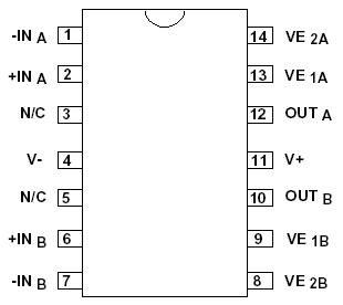
Features: • Factory pre-trimmed VOS• VOS = 25V @ IOS = 0.01pA• 5 V / s slew rate• EPAD ( Electrically Programmable Analog Device)• Rail-to-rail input/output• Each amplifier VOS can be user trimmed to a different Vos level (optional)• System level calibrat...
ALD2724E: Features: • Factory pre-trimmed VOS• VOS = 25V @ IOS = 0.01pA• 5 V / s slew rate• EPAD ( Electrically Programmable Analog Device)• Rail-to-rail input/output• Each...
SeekIC Buyer Protection PLUS - newly updated for 2013!
268 Transactions
All payment methods are secure and covered by SeekIC Buyer Protection PLUS.
The ALD2724E/ALD2724 is a dual monolithic operational amplifier with MOSFET input that has rail-to-rail input and output voltage ranges. The input voltage range and output voltage range are very close to the positive and negative power supply voltages. Typically the input voltage can be beyond positive power supply voltage V+ or the negative power supply voltage V- by up to 300mV. The output voltage swings to within 60mV of either positive or negative power supply voltages at rated load.
With high impedance load, the output voltage of the ALD2724E/ALD2724 approaches within 1mV of the power supply rails. This device is designed as an alternative to the popular J-FET input operational amplifier in applications where lower operating voltages, such as 9V battery or ±3.25V to ±5V power supplies are being used. The ALD2724E/ALD2724 offers high slew rate of 5.0V/ms.
The rail-to-rail input and output feature of the ALD2724E/ALD2724 expands signal voltage range for a given operating supply voltage and allows numerous analog serial stages to be implemented without losing operating voltage margin. The output stage is designed to drive up to 10mA into 400pF capacitive and 1.5KW resistive loads at unity gain and up to 4000pF at a gain of 5. Short circuit protection to either ground or the power supply rails is at approximately 15mA clamp current. Due to complementary output stage design, the output can source and sink 10mA into a load with symmetrical drive and is ideally suited for applications where push-pull voltage drive is desired.
For each of the operational amplifier, the offset voltage is trimmed on-chip to eliminate the need for external nulling in many applications. For precision applications, the output is designed to settle to 0.1% in 2ms. In large signal buffer applications, the operational amplifier can function as an ultra-high input impedance voltage follower/buffer that allows input and output voltage swings from positive to negative supply voltages. This feature of ALD2724E/ALD2724 is intended to greatly simplify systems design and eliminate higher voltage power supplies in many applications.
Each ALD2724E/ALD2724 operational amplifier features individual, user-programmable offset voltage trimming resulting in significantly enhanced total system performance and user flexibility. EPAD technology is an exclusive ALD design which has been refined for analog applications where precision voltage trimming is necessary to achieve a desired performance. It utilizes CMOS FETs as in-circuit elements for trimming of offset voltage bias characteristics with the aid of a personal computer under software control. Once programmed, the set parameters are stored indefinitely. EPAD offers the circuit designer a convenient and costeffective trimming solution for achieving the very highest amplifier/system performance.