ALD1502

Features: • High speed operation -- 2.5MHz typical oscillation at 5V• High discharge sinking current of 80mA at 5V• Guaranteed low operating supply voltage of 2V to 12V• Functional equivalent to and same pin-out as NE555/NE556 with greatly expanded high and low frequency ra...

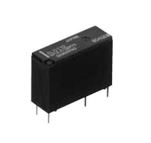
product image

ALD1502 Picture
SeekIC No. : 004279748 Detail

ALD1502: Features: • High speed operation -- 2.5MHz typical oscillation at 5V• High discharge sinking current of 80mA at 5V• Guaranteed low operating supply voltage of 2V to 12V• Func...

floor Price/Ceiling Price

Part Number:
ALD1502
Supply Ability:
5000

Price Break

  • Qty
  • 1~5000
  • Unit Price
  • Negotiable
  • Processing time
  • 15 Days
Total Cost: $ 0.00

SeekIC Buyer Protection PLUS - newly updated for 2013!

  • Escrow Protection.
  • Guaranteed refunds.
  • Secure payments.
  • Learn more >>

Month Sales

268 Transactions

Rating

evaluate  (4.8 stars)

Upload time: 2024/11/21

Payment Methods

All payment methods are secure and covered by SeekIC Buyer Protection PLUS.

Notice: When you place an order, your payment is made to SeekIC and not to your seller. SeekIC only pays the seller after confirming you have received your order. We will also never share your payment details with your seller.
Product Details

Description


Features:

• High speed operation -- 2.5MHz typical oscillation at 5V
• High discharge sinking current of 80mA at 5V
• Guaranteed low operating supply voltage of 2V to 12V
• Functional equivalent to and same pin-out as NE555/NE556 with greatly expanded high and low frequency ranges
• High speed, low power, monolithic CMOS technology
• Low supply current 50mA typical for ALD1502 and100mA typical for ALD2502
• Extremely low trigger, threshold and reset currents 10pA typical
• Operates in both monostable and astable modes
• Fixed 50% duty cycle or adjustable duty cycle
• CMOS, NMOS and TTL compatible input/output
• Low supply current spikes


Application

• High speed one-shot (monostable) pulse generation
• Precision timing
• Sequential timing
• Long delay timer
• Pulse width and pulse position modulation
• Missing pulse detector
• Frequency divider
• Synchronized timer


Specifications

Supply voltage, V+                                                                        13.2V
Input voltage range                                                                     -0.3V to V+ +0.3V
Power dissipation                                                                        600 mW
Operating temperature range PA, PB, SA, SB package                 0°C to + 70°C
                                                            DA, DB package                -55°C to +125°C
Storage temperature range                                                          -65°C to +150°C
Lead temperature, 10 seconds                                                    +260°C


Description

The ALD1502/ALD2502 timers are high performance single/dual monolithic timing circuits built with advanced silicon gate CMOS technology. They offer the benefits of high input impedance, thereby allowing smaller timing capacitors and a longer timing cycle; high speed, with typical cycle time of 400ns; low power dissipation for battery operated environment; reduced supply current spikes, allowing smaller and lower cost decoupling capacitors.

Each ALD1502/ALD2502 timer is capable of producing accurate time delays and oscillations in both monostable and astable operation, and operates in the one-shot (monostable) mode or 50% duty cycle free running oscillation mode with a single resistor and one capacitor. The inputs and outputs are fully compatible with CMOS, NMOS or TTL logic.

There are three matched internal resistors in ALD1502/ALD2502 (approximately 200KW each) that set the threshold and trigger levels at two-thirds and one-third respectively of V+. These levels can be adjusted by using the control terminal. When the trigger input is below the trigger level, the output is in the high state and sourcing 2mA. When the threshold input is above the threshold level at the same time the trigger input is above the trigger level, the internal flip-flop is reset, the output goes to the low state and sinks up to 10mA. The reset input overrides all other inputs and when it is active (reset voltage less than 1V), the output is in the low state.


Customers Who Bought This Item Also Bought

Margin,quality,low-cost products with low minimum orders. Secure your online payments with SeekIC Buyer Protection.
Test Equipment
Power Supplies - External/Internal (Off-Board)
RF and RFID
Resistors
View more