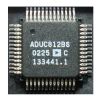
DescriptionThe ADuC7023 is a fully integrated, 1 MSPS, 12-bit data acquisition system, incorporating high performance multichannel ADCs, 16-bit/32-bit MCUs, and Flash/EE memory on a single chip.The ADC consists of up to 12 single-ended inputs. An additional four inputs are available but are multiplexed with the four DAC output pins. The ADuC7023 ADC can operate in single-ended or differential input modes. The ADC input voltage is 0 V to VREF. A low drift band gap reference, temperature sensor, and voltage comparator complete the ADC peripheral set.
Features of the ADuC7023 are:(1)external watch crystal; (2)external clock source up to 44 MHz; (3)41.78 MHz PLL with programmable divider; (4)Fully differential and single-ended modes; (5)0 V to VREF analog input range; (6)62 kB Flash/EE memory, 8 kB SRAM; (7)in-circuit download, JTAG-based debug; (8)software-triggered in-circuit reprogrammability; (9)vectored interrupt controller for FIQ and IRQ; (10)8 priority levels for each interrupt type; (11)interrupt on edge or level external pin inputs.The devices operate from an on-chip oscillator and a PLL,generating an internal high frequency clock of 41.78 MHz. This clock is routed through a programmable clock divider from which the MCU core clock operating frequency is generated.
The absolute maximum ratings of the ADuC7023 can be summarized as:(1)AVDD to IOVDD:-0.3 V to +0.3 V;(2)storage temperature range:-65 to +150;(3)operating temperature range:-40 to +125;(4)junction temperature:+150;(5)AGND to DGND:-0.3 V to +0.3 V.Stresses above those listed under Absolute Maximum Ratings may cause permanent damage to the device. This is a stress rating only; functional operation of the device at these or any other conditions above those indicated in the operational section of this specification is not implied.Exposure to absolute maximum rating conditions for extended periods may affect device reliability.However, the Thumb mode has two limitations. Thumb code typically requires more instructions for the same job. As a result, ARM code is usually best for maximizing the performance of time critical code. Also, the Thumb instruction set does not include some of the instructions needed for exception handling, which automatically switches the core to ARM code for exception handling.

 ADuC7023 Data Sheet


