Features: `Multiformat video decoder supports NTSC-(J, M, 4.43),`PAL-(B/D/G/H/I/M/N), SECAM`Integrates three 54 MHz, 10-bit ADCs`Clocked from a single 27 MHz crystal`Line-locked clock-compatible (LLC)`Adaptive Digital Line Length Tracking (ADLLT™), signal processing, and enhanced FIFO manage...
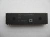
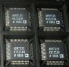
ADV7183B: Features: `Multiformat video decoder supports NTSC-(J, M, 4.43),`PAL-(B/D/G/H/I/M/N), SECAM`Integrates three 54 MHz, 10-bit ADCs`Clocked from a single 27 MHz crystal`Line-locked clock-compatible (LL...
SeekIC Buyer Protection PLUS - newly updated for 2013!
268 Transactions
All payment methods are secure and covered by SeekIC Buyer Protection PLUS.
Parameter | Rating |
AVDD to GND AVDD to AGND DVDD to DGND PVDD to AGND DVDDIO to DGND DVDDIO to AVDD PVDD to DVDD DVDDIO PVDD DVDDIO DVDD AVDD PVDD AVDD DVDD Digital Inputs Voltage to DGND Digital Output Voltage to DGND Analog Input to AGND Maximum Junction Temperature (TJ max) Storage Temperature Range Infrared Reflow Soldering (20 sec) |
4 V 4 V 2.2 V 2.2 V 4 V 0.3 V to +0.3 V 0.3 V to +0.3 V 0.3 V to +2 V 0.3 V to +2 V 0.3 V to +2 V 0.3 V to +2 V 0.3 V to DVDDIO + 0.3 V 0.3 V to DVDDIO + 0.3 V AGND 0.3 V to AVDD + 0.3 V 150°C 65°C to +150°C 260°C |
The ADV7183B integrated video decoder automatically detects and converts a standard analog baseband television signalcompatible with worldwide standards NTSC, PAL, and SECAM into 4:2:2 component video data-compatible with 16-/8-bit CCIR601/CCIR656.
The ADV7183B advanced and highly flexible digital output interface enables performance video decoding and conversion in linelocked clock-based systems. This makes the device ideally suited for a broad range of applications with diverse analog video characteristics, including tape-based sources, broadcast sources, security/surveillance cameras, and professional systems.
The ADV7183B 10-bit accurate A/D conversion provides professional quality video performance and is unmatched. This allows true 8-bit resolution in the 8-bit output mode.
The 12 analog input channels accept standard composite, S-Video, YPrPb video signals in an extensive number of combinations. ADV7183B AGC and clamp restore circuitry allow an input video signal peak-to-peak range of 0.5 V up to 1.6 V. Alternatively, these can be bypassed for manual settings.
The fixed 54 MHz clocking of the ADCs and datapath for all modes allows very precise, accurate sampling and digital filtering. The line-locked clock output allows the output data rate, timing signals, and output clock signals to be synchronous, asynchronous, or line locked even with ±5% line length variation. The output control signals of ADV7183B allow glueless interface connections in almost any application.
The ADV7183B modes are set up over a 2-wire, serial, bidirectional port (I2C-compatible).
The ADV7183B is fabricated in a 3.3 V CMOS process. Its monolithic CMOS construction ensures greater functionality with lower power dissipation. The ADV7183B is packaged in a small 80-lead LQFP Pb-free package.