Features: ·Complete suite of level shifters·Eight inverting and three complementary level shifters for LCD timing·High voltage edge detector·Integrated low offset buffer for VCOM drives high capacitive loads·MUXed input, low offset buffer for 2-level precharge drives high capacitive loads·High cur...
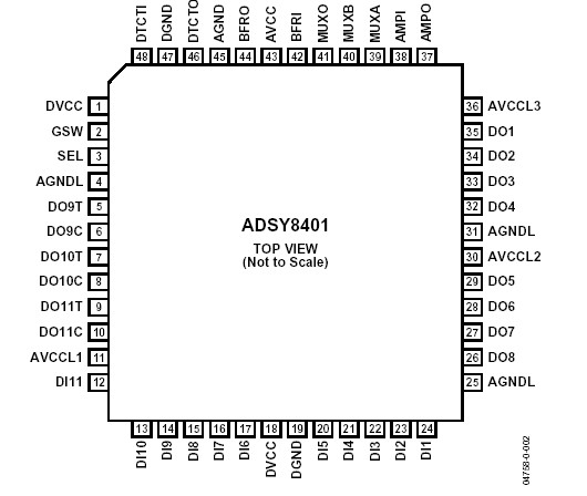
ADSY8401: Features: ·Complete suite of level shifters·Eight inverting and three complementary level shifters for LCD timing·High voltage edge detector·Integrated low offset buffer for VCOM drives high capacit...
SeekIC Buyer Protection PLUS - newly updated for 2013!
268 Transactions
All payment methods are secure and covered by SeekIC Buyer Protection PLUS.
Parameter | Rating |
Supply Voltages AVCC to AGND AVCCL to AGNDL AGND to AGNDL AGND to DGND DVCC to DGND Input Voltages Maximum Digital Input Voltages Minimum Digital Input Voltages Maximum Analog Input Voltages Minimum Analog Input Voltages Internal Power Dissipation1 LFCSP Package at 25°C, Ambient Operating Temperature Range Storage Temperature Range Lead Temperature Range (Soldering 10 s) |
18 V 18 V ±0.5 V ±0.5 V 4.5 V DVCC + 0.5 V DGND − 0.5 V AVCCx + 0.5 V AGNDx − 0.5 V 3.8 W 0°C to 85°C −65°C to +125°C 300°C |
The ADSY8401 provides fast, 3 V to 15 V level shifters for LCD panel timing signals. An integrated low offset analog buffer is capable of driving the high capacitive loads. A 2:1 MUX input, low offset buffer simplifies application of 2-level precharge signals. A high current buffer provides high slew rates for large capacitive loads.
The ADSY8401 is fabricated on ADI's fast, 26 V XFHV process, providing fast input logic, high voltage level shifters, and precision drive amplifiers on the same chip.
The ADSY8401 dissipates 576 mW nominal static power.
The ADSY8401 is offered in a 48-lead 7 mm * 7 mm LFCSP E-pad package and operates over the commercial temperature range of 0°C to 85°C.