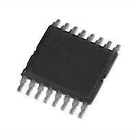
Features: • 1.25-MHz Sample Rate Serial Device• 10-Bit Resolution ADS7887• 8-Bit Resolution ADS7888• Zero Latency• 25-MHz Serial Interface• Supply Range: 2.35 V to 5.25 V• Typical Power Dissipation at 1.25 MSPS: 3.8 mW at 3-V V DD 8 mw at 5-V V DD̶...
ADS7888: Features: • 1.25-MHz Sample Rate Serial Device• 10-Bit Resolution ADS7887• 8-Bit Resolution ADS7888• Zero Latency• 25-MHz Serial Interface• Supply Range: 2.35 V...
SeekIC Buyer Protection PLUS - newly updated for 2013!
268 Transactions
All payment methods are secure and covered by SeekIC Buyer Protection PLUS.
US $2.66 - 2.66 / Piece
ADC (A/D Converters) 12B 1MSPS 4x2/2x2 Simu Sampling SAR
US $4.63 - 6.14 / Piece
ADC (A/D Converters) 12B 1MSPS 4x2/2x2 Simu Sampling SAR
US $2.85 - 3.78 / Piece
ADC (A/D Converters) Lo Pwr 12B 1-MHz Sgl Dual Unipolar Inp
UNIT | ||
+IN to AGND | 0.3 V to +V DD +0.3 V | |
+V DD to AGND | 0.3 V to 7.0 V | |
Digital input voltage to GND | 0.3V to (7.0 V) | |
Digital output to GND | 0.3 V to (+V DD + 0.3 V) | |
Operating temperature range | 40 ° C to 125 ° C | |
Storage temperature range | 65 ° C to 150 ° C | |
Junction temperature (T J Max) | 150 ° C | |
Power dissipation, SOT23 and SC70 packages | (T J Max T A )/ JA | |
JA Thermal impedance | SOT23 | 295.2 ° C/W |
SC70 | 351.3 ° C/W | |
Lead temperature, soldering | Vapor phase (60 sec) | 215 ° C |
Infrared (15 sec) | 220 ° C |
The ADS7887 is a 10-bit, 1.25-MSPS analog-to-digital converter (ADC), and the ADS7888 is a 8-bit, 1.25-MSPS ADC. The ADS7887 and ADS7888 include a capacitor based SAR A/D converter with inherent sample and hold. The serial interface in each device is controlled by the CS and SCLK signals for glueless connections with microprocessors and DSPs. The input signal is sampled with the falling edge of CS , and SCLK is used for conversion and serial data output.
The ADS7887 and ADS7888 operate from a wide supply range from 2.35 V to 5.25 V. The low power consumption of the devices make them suitable for battery-powered applications. The devices also include a power saving powerdown feature for when the devices are operated at lower conversion speeds.
The high level of the digital input to the ADS7887 and ADS7888 is not limited to device V DD . This means the digital input can go as high as 5.25 V when device supply is 2.35 V. This feature is useful when digital signals are coming from other circuit with different supply levels. Also this relaxes restriction on power up sequencing.
The ADS7887 and ADS7888 are available in 6-pin SOT23 and SC70 packages and are specified for operation from -40 ° C to 125 ° C.