Mounting Style
: SMD/SMT
Packaging
: Reel
Supply Voltage - Max
: 3.6 V
Input Type
: Voltage
Maximum Operating Temperature
: + 85 C
Number of Converters
: 1
Number of ADC Inputs
: 1
Resolution
: 14 bit
Supply Voltage - Min
: 3 V
Architecture
: Pipelined
Voltage Reference
: Internal, External
Interface Type
: LVDS, Parallel
SNR
: 72.3 dB
Conversion Rate
: 250000 KSPs
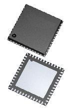
Package / Case
: QFN EP
Maximum Power Dissipation
: 730 mW
Pinout
 Description
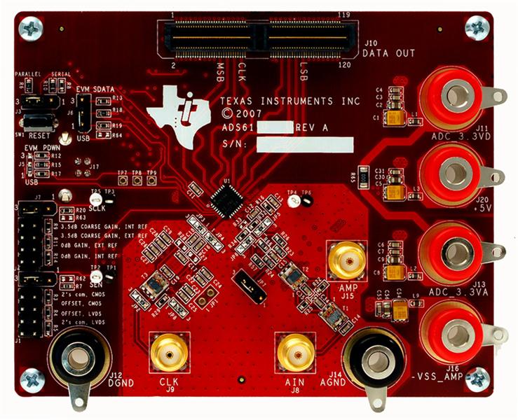
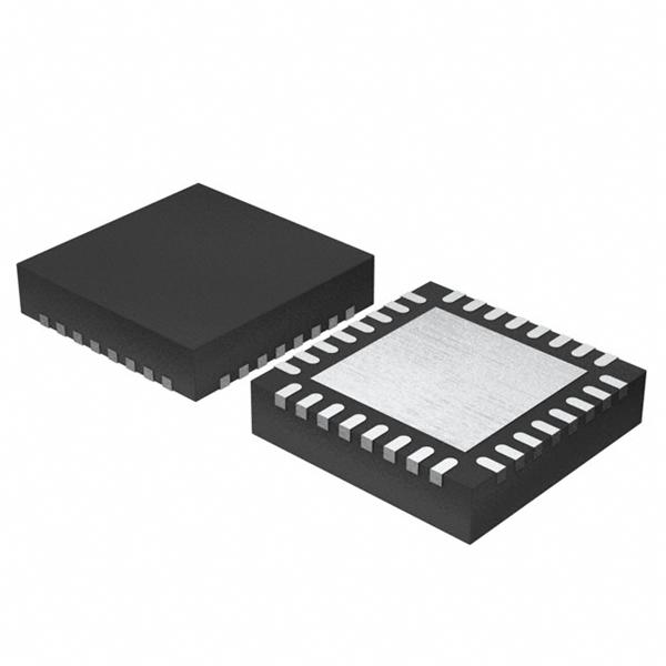
The ADS61B49IRGZT is designed as a 14-bit A/D converter with a sampling rate up to 250MSPS. It combines high dynamic performance and low power consumption in a compact 48-QFN package. An integrated analog buffer makes it well-suited for multi-carrier, wide bandwidth communications applications. The buffer maintains constant performance and input impedance across a wide frequency range.
ADS61B49IRGZT has ten features. (1)Integrated high impedance analog input buffer. (2)Maximum sample rate 250 MSPS. (3)14-bit resolution. (4)790mW total power dissipation at 250 MSPS. (5)Double data rate (DDR) LVDS and parallel CMOS output options. (6)Programmable fine gain up to 6dB for SNR/SFDR trade-off and 1Vpp full-scale operation. (7)DC offset correction. (8)Supports input clock amplitude down to 400mVpp differential. (9)48-QFN package (7mmx7mm). (10)Pin compatible with ADS6149 family. Those are all the main features.
Some absolute maximum ratings of ADS61B49IRGZT have been concluded into several points as follow. (1)Its supply voltage AVDD would be from -0.3V to 3.9V. (2)Its supply voltage DRVDD would be from -0.3V to 2.2V. (3)Its voltage between AGND and DRGND would be from -0.3V to 0.3V. (4)Its voltage between AVDD to DRVDD (when AVDD leads DRVDD) would be from 0V to 3.3V. (5)Its voltage between DRVDD to AVDD (when DRVDD leads AVDD) would be from -1.5V to 1.8V. (6)Its voltage applied to analog input pins would be from -0.3V to minimum (3.6, AVDD+0.3). (7)Its operating free-air temperature range would be from -40°C to 85°C. (8)Its max operating junction temperature would be 125°C. (9)Its storage temperature range would be from -65°C to 150°C. And so on. It should be noted that stresses above those listed in absolute maximum ratings may cause permanent damage to device.
Also some electrical characteristics of ADS61B49IRGZT are concluded as follow. (1)Its differential input voltage range would be typ 2Vpp. (2)Its differential input resistance would be typ 10kohms. (3)Its differential input capacitance would be typ 2pF. (4)Its analog input bandwidth would be typ 750MHz. (5)Its analog input common current (per input pin) would be typ 2uA. And so on. If you have any question or suggestion or want to know more information about ADS61B49IRGZT, please contact us for details. Thank you!
Parameters: | Technical/Catalog Information | ADS61B49IRGZT |
| Vendor | Texas Instruments (VA) |
| Category | Integrated Circuits (ICs) |
| Number of Bits | 14 |
| Package / Case | 48-VQFN |
| Data Interface | Serial/Parallel |
| Packaging | Digi-Reel? |
| Sampling Rate (Per Second) | 250M |
| Operating Temperature | -40°C ~ 85°C |
| Voltage Supply Source | Analog and Digital |
| Number of Inputs and Type | 1 Differential, Unipolar |
| Number of Converters | 1 |
| Power Dissipation (Max) | 790mW |
| Lead Free Status | Lead Free |
| RoHS Status | RoHS Compliant |
| Other Names | ADS61B49IRGZT
ADS61B49IRGZT
296 24045 6 ND
296240456ND
296-24045-6
|
 ADS61B49IRGZT Data Sheet