ADS5413

Features: 12-Bit Resolution65-MSPS Maximum Sample Rate2-Vpp Differential Input Range3.3-V Single Supply Operation1.8-V to 3.3-V Output Supply400-mW Total Power DissipationTwoís Complement Output FormatOn-Chip S/H and Duty Cycle Adjust CircuitInternal or External Reference48-Pin TQFP Package With P...

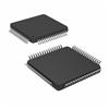
product image

ADS5413 Picture
SeekIC No. : 004277158 Detail

ADS5413: Features: 12-Bit Resolution65-MSPS Maximum Sample Rate2-Vpp Differential Input Range3.3-V Single Supply Operation1.8-V to 3.3-V Output Supply400-mW Total Power DissipationTwoís Complement Output For...

floor Price/Ceiling Price

Part Number:
ADS5413
Supply Ability:
5000

Price Break

  • Qty
  • 1~5000
  • Unit Price
  • Negotiable
  • Processing time
  • 15 Days
Total Cost: $ 0.00

SeekIC Buyer Protection PLUS - newly updated for 2013!

  • Escrow Protection.
  • Guaranteed refunds.
  • Secure payments.
  • Learn more >>

Month Sales

268 Transactions

Rating

evaluate  (4.8 stars)

Upload time: 2024/6/6

Payment Methods

All payment methods are secure and covered by SeekIC Buyer Protection PLUS.

Notice: When you place an order, your payment is made to SeekIC and not to your seller. SeekIC only pays the seller after confirming you have received your order. We will also never share your payment details with your seller.
Product Details

Description


Features:

12-Bit Resolution
65-MSPS Maximum Sample Rate
2-Vpp Differential Input Range
3.3-V Single Supply Operation
1.8-V to 3.3-V Output Supply
400-mW Total Power Dissipation
Twoís Complement Output Format
On-Chip S/H and Duty Cycle Adjust Circuit
Internal or External Reference
48-Pin TQFP Package With PowerPad (7 mm x 7 mm body size)
64.5-dBFS SNR and 72-dBc SFDR at 65 MSPS and 190-MHz Input
Power-Down Mode
Single-Ended or Differential Clock
1-GHz −3-dB Input Bandwidth


Application

High IF Sampling Receivers
Medical Imaging
Portable Instrumentation


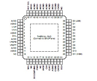
Pinout

  Connection Diagram


Specifications

  UNITS
Supply voltage range AVDD measured with respect to AGND −0.3 V to 3.9 V
OVDD measure with respect to OGND −0.3 V to 3.9 V
Digital input, measured with respect to AGND −0.3 V to AVDD + 0.3 V
Reference inputs Vrefb or Vreft, measured with respect to AGND −0.3 V to AVDD + 0.3 V
Analog inputs Vinp or Vinn, measured with respect to AGND −0.3 V to AVDD + 0.3 V
Maximum storage temperature 150°C
Soldering reflow temperature 235°C


Description

The ADS5413 is a low power, 12-bit, 65-MSPS, CMOS pipeline analog-to-digital converter (ADC) that operates from a single 3.3-V supply, while offering the choice of digital output levels from 1.8 V to 3.3 V. The low noise, high linearity, and low clock jitter makes the ADC well suited for high-input frequency sampling applications. On-chip duty cycle adjust circuit allows the use of a non-50% duty cycle. This can be bypassed for applications requiring low jitter or asynchronous sampling. The device can also be clocked with single ended or differential clock, without change in performance. The internal reference can be bypassed to use an external reference to suit the accuracy and low drift requirements of the application.

The ADS5413 is specified over full temperature range (−40°C to +85°C).


Customers Who Bought This Item Also Bought

Margin,quality,low-cost products with low minimum orders. Secure your online payments with SeekIC Buyer Protection.
Test Equipment
Industrial Controls, Meters
Soldering, Desoldering, Rework Products
Power Supplies - External/Internal (Off-Board)
Line Protection, Backups
Circuit Protection
View more