Features: ·Maximum Sample Rate: 65MSPS
·12-Bit Resolution
·No Missing Codes
·Power Dissipation: 996mW
·CMOS Technology
·Simultaneous Sample-and-Hold
·70.5dB SNR at 10MHz IF
·Internal and External References
·3.3V Digital/Analog Supply
·Serialized LVDS Outputs
·Integrated Frame and Synch Patterns
·MSB and LSB First Modes
·Option to Double LVDS Clock Output Currents
·Pin- and Format-Compatible Family
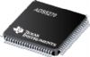
·TQFP-80 PowerPAD™ PackageApplication·Portable Ultrasound Systems
·Tape Drives
·Test Equipment
·Optical NetworkingPinout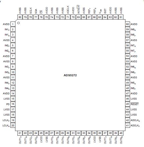 Specifications
Supply Voltage Range, AVDD . . . . . . . . . . . . . . . . −0.3V to 3.8V
Supply Voltage Range, LVDD . . . . . . . . . .. . . . . . . −0.3V to 3.8V
Voltage Between AVSS and LVSS . . . . . . . . . . . . . −0.3V to 0.3V
Voltage Between AVDD and LVDD . . . . . . . . . . . . −0.3V to 0.3V
Voltages Applied to External REF Pins . . . . . . . . . −0.3V to 2.4V
All LVDS Data and Clock Outputs . . . . . . . .. . . . . . −0.3V to 2.4V
Analog Input Pins . . . . . . . . . . . . . . . . . . . . . . . . −0.3V to 2.7V
Peak Total Input Current (all inputs) . . . . . . . . . . . . . . . . −30mA
Operating Free-Air Temperature Range, TA . . . . . . −40 to 85
Lead Temperature 1.6mm (1/16 from case for 10s) . . . . 220
(1) Stresses above these ratings may cause permanent damage. Exposure to absolute maximum conditions for extended periods may degrade device reliability. These are stress ratings only, and functional operation of the device at these or any other conditions beyond those specified is not supported.
DescriptionThe ADS5272 is a high-performance, 65MSPS, 8-channel, parallel analog-to-digital converter (ADC). Internal references are provided, simplifying system design requirements. Low power consumption allows for the highest of system integration densities. Serial LVDS (low-voltage differential signaling) outputs reduce the number of interface lines and package size.
An integrated phase lock loop multiplies the incoming ADC sampling clock by a factor of 12. This 12x clock is used in the process of serializing the data output from each channel. The 12x clock is also used to generate a 1x and a 6x clock, both of which are transmitted as LVDS clock outputs. The 6x clock is denoted by the differential pair LCLKP and LCLKN, while the 1x clock is denoted by ADCLKP and ADCLKN. The word output of each ADC channel can be transmitted either as MSBor LSB first. The bit coinciding with the rising edge of the 1x clock output is the first bit of the word. Data of ADS5272 is to be latched by the receiver on both the rising and falling edges of the 6x clock.
The ADS5272 provides internal references, or can optionally be driven with external references. Best performance can be achieved through the internal reference mode. The device is available in a TQFP-80 PowerPAD package and is specified over a −40°C to +85°C operating range.

 ADS5272 Data Sheet