Features: 3.3V Single-Supply Operation
Dual Simultaneous Sample-and-Hold Inputs
Differential or Single-Ended Analog Inputs
Programmable Gain Amplifier: 0dB to 18dB
Separate Serial Control Interface
Single or Dual Parallel Bus Output
60dB SNR at fIN = 10.5MHz
73dB SFDR at fIN = 10.5MHz
Low Power: 275mW
300MHz Analog Input Bandwidth
3.3V TTL/CMOS-Compatible Digital I/O
Internal or External Reference
Adjustable Reference Input Range
Power-Down (Standby) Mode
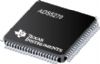
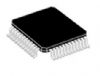
TQFP-48 Package
ApplicationDigital Communications (Baseband Sampling)
Portable Instrumentation
Video ProcessingPinout Specifications
Supply Voltage: AVDD to AGND, DVDD to DGND . . . . . . . . . . . . . . .-0.5V to 3.6V
Supply Voltage: AVDD to DVDD, AGND to DGND . . . . . . . . . . . . . . .-0.5V to 0.5V
Digital Input Voltage Range to DGND . . . . . . . . . . . . . . . .-0.5V to DVDD + 0.5V
Analog Input Voltage Range to AGND . . . . . . . . . . . . . . . . -0.5V to AVDD + 0.5V
Digital Output Voltage Applied from Ext. Source to DGND . .-0.5V to DVDD + 0.5V
Reference Voltage Input Range to AGND: VREFT , VREFB . . . -0.5V to AVDD + 0.5V
Operating Free¨Air Temperature Range, TA (ADS5204I) . . . . . . . .-40 to +85
Storage Temperature Range, TSTG . . . . . .. . . . . . . . . .. . . . . . . . .-65 to +150
Soldering Temperature 1.6mm (1/16 inch) from case for 10 seconds . . . . .300
Description The ADS5204 is a dual 10-bit, 40MSPS Analog-to-Digital Converter (ADC). It simultaneously converts each analog input signal into a 10-bit, binary coded digital word up to a maximum sampling rate of 40MSPS per channel. All digital inputs and outputs are 3.3VTTL/CMOS compat-ible.
An innovative dual pipeline architecture implemented in a CMOS process and the 3.3V supply results in very low power dissipation. In order to provide maximum flexibil-ity, both top and bottom voltage references can be set from user-supplied voltages. Alternatively, if no external references are available, the on-chip internal refer-ences can be used. Both ADCs share a common refer-ence to improve offset and gain matching. If external reference voltage levels are available, the internal refer-ences can be powered down independently from the rest of the ADS5204, resulting in even greater power savings.
The ADS5204 also features dual, onboard Programmable Gain Amplifiers (PGAs) that allow a setting of 0dB to 18dB to adjust the gain of each set of inputs in order to match the amplitude of the incoming signal.
The ADS5204 is characterized for operation from -40 to +85 and is available in a TQFP-48 package.

 ADS5204 Data Sheet