Features: `11 LDOs Optimized for Specific CDMA Subsystems
`4 Backup LDOs for Standby Mode Operation
`Ultra Low Standby Supply Current
`High Accuracy Battery Charger (0.7%)
`3 Li-Ion Battery Charge Modes
5 mA Precharge
Low Current Charge
Full Current Charge
`Integrated RTC
`Ambient Temperature: 30�C to +85�C
`64-Lead 7 mm * 7 mm * 1 mm TQFP PackageApplication·CDMA/CDMA2000/PCS HandsetsPinout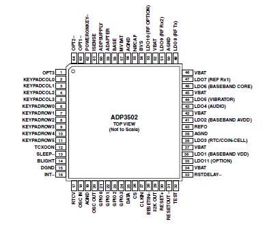 Specifications
Voltage on ADAPTER, ADPSUPPLY Pin
to GND . . . . . . . . . . . . . . . . . . . . . . . . . . . .. ... .0.3 V, 15 V
Voltage on VBAT Pin to GND . . . . . . . . . . . .. . .0.3 V, +6.5 V
Voltage on Pins 613, 2128
to GND . . . . . . . . . . . . . . . . . . . . . . .. 0.3 V, VLDO1 + 0.3 V
Voltage on Pins 1, 6264 . . . . . . . . . . ..0.3 V, VBAT + 0.3 V
Voltage on Pins 20, 32 . . . . . . . . . . . . . 0.3 V, VRTCV + 0.3 V
Voltage on Pin 60 . . . . . . . . . . . . .... 0.3 V, VADAPTER + 0.3 V
Voltage on Pins 25, 14, 30, 31, 33 . . . . .. . .. 0.3 V, +6.5 V
Storage Temperature Range . . . . . . . . . . .65°C to +150°C
Operating Temperature Range . . . . . . . . . . 30°C to +85°C
Maximum Junction Temperature . . . . . . . . . ... . . . . . . . 125°C
JA Thermal Impedance (TQFP-64)
(2-Layer Board) . . . . . . . . . . . . . . . . . . . . . . . . . . . .87.4°C/W
JA Thermal Impedance (TQFP-64)
(4-Layer Board) . . . . . . . . . . . . . . . . . . . . . . . . . .. . 56.2°C/W
Lead Temperature Range
(Soldering, 60 sec) . . . . . . . . . . . . . . . . . . . . . . . . . . . 300°C
*Stresses above those listed under Absolute Maximum Ratings may cause permanent
damage to the device. This is a stress rating only; functional operation of the
device at these or any other conditions above those listed in the operational
sections of this specification is not implied. Exposure to absolute maximum rating
conditions for extended periods may affect device reliability. Absolute maximum
ratings apply individually only, not in combination. Unless otherwise specified all
other voltages are referenced to GND.
DescriptionThe ADP3502 is a multifunction chip optimized for CDMA-1x cell phone power management. It offers a total power solution for the handset baseband and RF section, including LDOs to power 11 subsystems. Also integrated are a real-time clock (RTC), serial bus interface, and charging control for Li-Ion/ Li-Polymer batteries. Sophisticated controls are available for power-up during battery charging, keypad interface, GPIO/INT function, and RTC function.
The ADP3502 is optimized for CDMA handsets powered by single-cell Li-Ion batteries. Its high level of integration significantly reduces the design effort, number of discrete components, and solution size/cost. The main-sub LDO structure reduces the standby current consumption, and as a result, greatly extends the standby time of the phone. System operation has been proven to be fully compatible with MSM51xx-based designs.
The ADP3502 comes in a 64-lead 7 mm * 7 mm * 1 mm TQFP package and is specified over a wide temperature range of 30°C to +85°C.

 ADP3502 Data Sheet