Features: Optimally Compensated Active Voltage Positioning with Gain and Offset Adjustment (ADOPT™) for Superior Load Transient ResponseComplies with VRM 8.4 Specifications with LowestSystem Cost4-Bit Digitally Programmable 1.3 V to 2.05 V OutputN-Channel Synchronous Buck DriverTwo On-Board ...
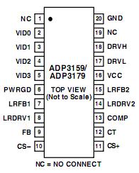
ADP3159: Features: Optimally Compensated Active Voltage Positioning with Gain and Offset Adjustment (ADOPT™) for Superior Load Transient ResponseComplies with VRM 8.4 Specifications with LowestSystem C...
SeekIC Buyer Protection PLUS - newly updated for 2013!
268 Transactions
All payment methods are secure and covered by SeekIC Buyer Protection PLUS.
The ADP3159 and ADP3179 are highly efficient output synchronous buck switching regulator controllers optimized for converting a 5 V main supply into the core supply voltage required by high-performance processors. These devices use an internal 4-bit DAC to read a voltage identification (VID) code directly from the processor, which is used to set the output voltage between 1.3 V and 2.05 V. ADP3159 and ADP3179 use a current mode, constant off-time architecture to drive two N-channel MOSFETs at a programmable switching frequency that can be optimized for regulator size and efficiency.
The ADP3159 and ADP3179 also use a unique supplemental regulation technique called Analog Devices Optimal Positioning Technology (ADOPT) to enhance load transient performance. Active voltage positioning results in a dc/dc converter that meets the stringent output voltage specifications for high performance processors, with the minimum number of output capacitors and smallest footprint. Unlike voltage-mode and standard current-mode architectures, active voltage positioning adjusts the output voltage as a function of the load current so it is always optimally positioned for a system tran sient. The devices also provide accurate and reliable short circuit protection and adjustable current limiting. They also include an integrated overvoltage crowbar function to protect the microprocessor from destruction in case the core supply exceeds the nominal programmed voltage by more than 20%. The ADP3159 and ADP3179 contain two fixed-output voltage linear regulator controllers that are designed to drive external N-channel MOSFETs. The outputs are internally fixed at 2.5 V and 1.8 V in the ADP3159, while the ADP3179 provides adjustable output, which is set using an external resistor divider. These linear regulators are used to generate the auxiliary voltages (AGP, GTL, etc.) required in most motherboard designs, and have been designed to provide a high bandwidth load-transient response. The ADP3159 and ADP3179 are specified over the commercial temperature range of 0°C to 70°C and are available in a 20-lead TSSOP package.