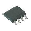
Features: `Wide bias voltage range 3.0 V to 18 V Wide power stage input range 1 V to 24 V Wide output voltage range: 0.6 V to 85% of input voltage ±0.85% accuracy at 0oC to 70oC
`All N-channel MOSFET design for low cost
`Fixed-frequency operation at 300 kHz, 600 kHz, or resistor adjustable 300 kHz to 600 kHz Clock output for ynchronizing other controllers
`No current sense resistor required
`Internal linear regulator
`Voltage tracking for sequencing
`Soft start and thermal overload protection
`Overvoltage and undervoltage power-good indicator
`15 A shutdown supply current
`Available in a 20-lead QSOP
Application·Telecom and networking systems
·Base station power
·Set-top boxes, game consoles
·Printers and copiers
·Medical imaging systems DSP and microprocessor core power supplies DDR terminationPinout Specifications
|
Parameter |
Rating |
|
IN, TRK
EN
PV, SYNC, FREQ, COMP, SS, FB, PGOOD, CLKSET, CLKOUT, VREG
BST-to-GND, SW-to-GND
BST-to-SW
BST-to-GND, SW-to-GND, 50 ns transients
SW-to-GND, 30 ns negative transients
CSL-to-GND
DH-to-GND
DL-to-PGND
PGND-to-GND
JA, 20-Lead QSOP on a Multilayer PCB (Natural Convection)1
Operating Junction Temperature2
Storage Temperature
Maximum Soldering Lead Temperature |
−0.3 V to +20 V
−0.3 V < IN + 0.3 V
−0.3 V to +6 V
−0.3 V to +30 V
−0.3 V to +6 V
+38 V
−7 V
−1 V to +30 V
(SW − 0.3 V) to (BST + 0.3 V)
−0.3 V to (PV + 0.3 V)
±2 V
83°C/W
−40°C to +125°C
−65°C to +150°C
260°C |
1 Junction-to-ambient thermal resistance ( JA) of the package was calculated or simulated on a multilayer PCB.
2 The ADP1828 can be damaged when the junction temperature limits are exceeded. Monitoring ambient temperature does not guarantee that TJ is within the specified temperature limits. In applications with moderate power dissipation and low PCB thermal resistance, the maximum ambient temperature can exceed the maximum limit as long as the junction tem-perature is within specification limits. The junction temperature, T J, of the device is dependent on the ambient temperature, T A, the power dissipation of the device, P D, and the junction to ambient thermal resistance of the package, JA. Maximum junction temperature is calculated from the ambient temperature and power dissipation using the formula TJ = TA + PD * JA. Stresses above those listed under Absolute Maximum Ratings may cause permanent damage to the device. This is a stress rating only; functional operation of the device at these or any other conditions above those indicated in the operational section of this specification is not implied. Exposure to absolute maximum rating conditions for extended periods may affect device reliability.
Absolute maximum ratings apply individually only, not in combination. Unless otherwise specified all other voltages are referenced to GND.
DescriptionThe ADP1828 is a versatile and synchronous PWM voltage mode buck controller. It drives an all N-channel power stage to regulate an output voltage as low as 0.6 V to 85% of the input voltage and is sized to handle large MOSFETs for point-of-load regulators.
The ADP1828 is ideal for a wide range of high power applications, such as DSP and processor core I/O power, and general-purpose power in telecommunications, medical imaging, PC, gaming, and industrial applications. It operates from input bias voltages of 3 V to 18 V with an internal LDO that generates a 5 V output for input bias voltages greater than 5.5 V. The ADP1828 operates at a pin-selectable, fixed switching frequency of either 300 kHz or 600 kHz, or at any frequency between 300 kHz and 600 kHz with a resistor. The switching frequency can also be synchronized to an external clock up to 2* the part's nominal oscillator frequency. The clock output can be used for synchronizing additional ADP1828s (or the ADP1829 controllers), thus eliminating the need for an external clock source. It includes soft start protection to limit any inrush current from the input supply during startup, reverse current protection during soft start for a precharged output, as well as a unique adjustable lossless current-limit scheme utilizing external MOSFET RDSON sensing.
For applications requiring power-supply sequencing, the ADP1828 provides a tracking input that allows the output voltage to track during startup, shutdown, and faults. The
additional supervisory and control features include thermal overload, undervoltage lockout, and power good.
The ADP1828 operates over the −40°C to +125°C junction temperature range and is available in a 20-lead QSOP.

 ADP1828 Data Sheet


