PinoutSpecifications Vout Preset 16 Presets From 0.75-3.3V,Soft Start Vout Adj Range n/a Vin Range (Vmin to Vmax) 2.5 to 5.5 Iout (max) 1A Supply Current 1.55mA Vdropout @ Rated Iout 345mV to 365mV Vout Total Acc 1.5% @ 0.1 mA - Iout max Package LFCSP-8,S...
ADP1706: PinoutSpecifications Vout Preset 16 Presets From 0.75-3.3V,Soft Start Vout Adj Range n/a Vin Range (Vmin to Vmax) 2.5 to 5.5 Iout (max) 1A Supply Current 1.55mA Vdropout ...
SeekIC Buyer Protection PLUS - newly updated for 2013!
268 Transactions
All payment methods are secure and covered by SeekIC Buyer Protection PLUS.
Vout Preset | 16 Presets From 0.75-3.3V,Soft Start |
Vout Adj Range | n/a |
Vin Range (Vmin to Vmax) | 2.5 to 5.5 |
Iout (max) | 1A |
Supply Current | 1.55mA |
Vdropout @ Rated Iout | 345mV to 365mV |
Vout Total Acc | 1.5% @ 0.1 mA - Iout max |
Package | LFCSP-8,SOIC-8 |
# of Outputs | 1 |
Line Regulation | n/a |
Load Regulation | n/a |
Shutdown | Yes |
Operating Temp Range | -40 to +125 |
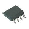
The ADP1706 is designed as one kind of 1 A, low dropout, CMOS linear regulator device that can be used in wide range of applications such as (1)Notebook computers; (2)Memory components; (3)Telecommunications equipment; (4)Network equipment; (5)DSP/FPGA/microprocessor supplies; (6)Instrumentation equipment/data acquisition systems. And this device is available in an 8-lead, exposed paddle SOIC package and an 8-lead, 3 mm * 3 mm exposed paddle LFCSP.
Features of the ADP1706 are:(1)Stable with small 4.7 F ceramic output capacitor; (2)Excellent load/line transient response; (3)Current limit and thermal overload protection; (4)Logic-controlled enable; (5)Available in an 8-lead, exposed paddle SOIC and 3 mm * 3 mm, 8-lead exposed paddle LFCSP; (6)Maximum output current: 1 A; (7)Input voltage range: 2.5 V to 5.5 V; (8)Low shutdown current: <1 A; (9)Low dropout voltage: 345 mV @ 1 A load; (10)Initial accuracy: ±1%; (11)Accuracy over line, load, and temperature: ±2.5%.
The absolute maximum ratings of the ADP1706 can be summarized as:(1)VIN to GND: -0.3 V to +6.0 V;(2)VOUT to GND: -0.3 V to VIN;(3)EN to GND: -0.3 V to +6.0 V;(4)Storage Temperature Range: -65°C to +150°C;(5)Operating Junction Temperature Range: -40°C to +125°C;(6)Operating Ambient Temperature Range: -40°C to +85°C;(7)Soldering Conditions: JEDEC J-STD-020. If you want to know more information about the ADP1706, please download the datasheet in www.seekic.com or www.chinaicmart.com .