ADN2890

Features: SFP reference design available Input sensitivity: 3 mV p-p 80 ps rise/fall times CML outputs: 700 mV p-p differential Programmable LOS detector: 2 mV to 13 mV Rx signal strength indicator (RSSI):SFF-8472 compliant average power measurement Single-supply operation: 3.3 V Low power dissipa...

product image

ADN2890 Picture
SeekIC No. : 004276227 Detail

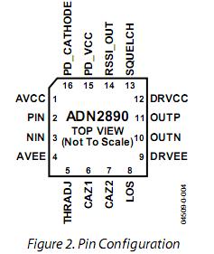
ADN2890: Features: SFP reference design available Input sensitivity: 3 mV p-p 80 ps rise/fall times CML outputs: 700 mV p-p differential Programmable LOS detector: 2 mV to 13 mV Rx signal strength indicator ...

floor Price/Ceiling Price

Part Number:
ADN2890
Supply Ability:
5000

Price Break

  • Qty
  • 1~5000
  • Unit Price
  • Negotiable
  • Processing time
  • 15 Days
Total Cost: $ 0.00

SeekIC Buyer Protection PLUS - newly updated for 2013!

  • Escrow Protection.
  • Guaranteed refunds.
  • Secure payments.
  • Learn more >>

Month Sales

268 Transactions

Rating

evaluate  (4.8 stars)

Upload time: 2024/5/28

Payment Methods

All payment methods are secure and covered by SeekIC Buyer Protection PLUS.

Notice: When you place an order, your payment is made to SeekIC and not to your seller. SeekIC only pays the seller after confirming you have received your order. We will also never share your payment details with your seller.
Product Details

Description


Features:

SFP reference design available
Input sensitivity: 3 mV p-p
80 ps rise/fall times
CML outputs: 700 mV p-p differential
Programmable LOS detector: 2 mV to 13 mV
Rx signal strength indicator (RSSI):SFF-8472 compliant average power measurement
Single-supply operation: 3.3 V
Low power dissipation: 130 mW
Available in space-saving 3 mm × 3 mm 16-lead LFCSP


Application

SFP/SFF/GBIC optical transceivers
OC-3/12/48, GbE, Fibre Channel receivers
10GBASE-LX4 transceivers
WDM transponders


Pinout

  Connection Diagram

ADN2890 Diagram


Specifications

Parameter Rating
Supply Voltage 4.2 V
Minimum Input Voltage (All Inputs) VEE − 0.4 V
Maximum Input Voltage (All Inputs) VCC + 0.4 V
Storage Temperature −65°C to +155°C
Operating Temperature Range −40°C to +85°C
Lead Temperature Range (Soldering 10 s) 300°C
Junction Temperature 125°C


Data Rate (Gb/s) 3.2Gbps
Voltage Supply (V) +3.3V
Package 3x3 mm LFCSP
Input Sensitivity (mVp-p) 3mV p-p
Power Dissipation (mW) 130mW
Jitter (rms) 2.4s rms
Output Levels (mVpp diff) 700mV p-p
Squelch X
LOS 3mV to 12mV
RSSI X


Description

The ADN2890 is a high gain, limiting amplifier optimized foruse in SONET, Gigabit Ethernet (GbE), and Fibre Channeloptical receivers that accept input levels of up to 2.0 V p-p differential and have 3 mV p-p differential input sensitivity. The product provides the receiver functions of quantization and loss of signal (LOS) detection. The ADN2890 can easily operate at up to 3.2 Gb/s to support LX4 transceivers.The limiting amplifier also measures average received power based on a direct measurement of the photodiode current with better than 1 dB of accuracy over the entire input range of the receiver. This eliminates the need for external average Rx power detection circuitry in SFF-8472 compliant optical transceivers.

The ADN2890 limiting amplifier operates from a single 3.3 Vsupply, has low power dissipation, and is available in a spacesaving 3 mm × 3 mm 16-lead lead frame chip scale package (LFCSP).


Customers Who Bought This Item Also Bought

Margin,quality,low-cost products with low minimum orders. Secure your online payments with SeekIC Buyer Protection.
Cable Assemblies
Undefined Category
Computers, Office - Components, Accessories
Hardware, Fasteners, Accessories
Optical Inspection Equipment
LED Products
View more