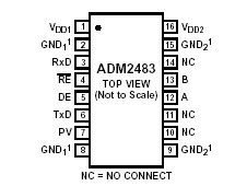
Features: RS-485 transceiver with electrical data isolation Complies with ANSI TIA/EIA RS-485-A and ISO 8482: 1987(E) 500 kbps data rate Slew rate-limited driver outputs Low power operation: 2.5 mA max Suitable for 5 V or 3 V operations (VDD1) High common-mode transient immunity: >25 kV/s True...
ADM2483: Features: RS-485 transceiver with electrical data isolation Complies with ANSI TIA/EIA RS-485-A and ISO 8482: 1987(E) 500 kbps data rate Slew rate-limited driver outputs Low power operation: 2.5 mA...
SeekIC Buyer Protection PLUS - newly updated for 2013!
268 Transactions
All payment methods are secure and covered by SeekIC Buyer Protection PLUS.
Parameter | Rating |
VDD1 VDD2 Digital Input Voltage (DE, RE, TxD) Digital Output Voltage RxD Driver Output/Receiver Input Voltage ESD Rating: Contact (Human Body Model) (A, B Pins) Operating Temperature Range Storage Temperature Range Average Output Current per Pin JA Thermal Impedance Lead Temperature Soldering (10 sec) Vapor Phase (60 sec) Infrared (15 sec) |
−0.5 V to +7 V |
Max Operating Temp (°C) | 85Deg |
Insulation Rating (kVrms) | 2.5kV rms |
# Ch | 1 |
Isolated Output (V)min | 1.5V |
Isolated Output (V)max | 5V |
Output Default State | Z |
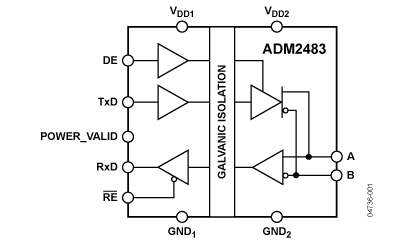
The ADM2483 differential bus transceiver is an integrated, galvanically isolated component designed for bidirectional data communication on balanced, multipoint bus transmission lines. It complies with ANSI EIA/TIA-485-A and ISO 8482: 1987(E). Using Analog Devices' iCoupler technology, the ADM2483 combines a 3-channel isolator, a three-state differential line driver, and a differential input receiver into a single package. The logic side of ADM2483 is powered with either a 5 V or 3 V supply, and the bus side uses a 5 V supply only.
The ADM2483 is slew-limited to reduce reflections with improperly terminated transmission lines. The controlled slew rate limits the data rate to 500 kbps. The device's input impedance is 96 kΩ, allowing up to 256 transceivers on the bus. Its driver has an active-high enable feature. The driver differential outputs and receiver differential inputs are connected internally to form a differential I/O port. When the driver is disabled or when VDD1 or VDD2 = 0 V, this imposes minimal loading on the bus. An active-high receiver disable feature, which causes the receive output to enter a high impedance state, is provided as well.
The ADM2483 receiver inputs have a true fail-safe feature that ensures a logic-high receiver output level when the inputs are open or shorted. This guarantees that the receiver outputs are in a known state before communication begins and at the point when communication ends.
Current limiting and thermal shutdown features of ADM2483 protect against output short circuits and bus contention situations that might cause excessive power dissipation. The part is fully specified over the industrial temperature range and is available in a 16-lead, wide body SOIC package.