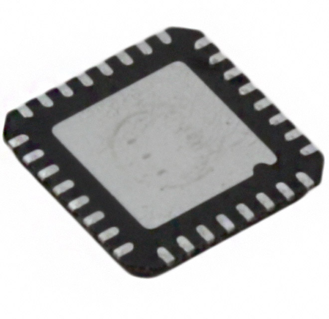
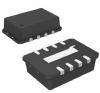
DescriptionThe ADL5535 also provides extremely flat gain and P1dB over frequency, which are stable over temperature, power supply, and from device to device. The device is internally matched to 50 at the input and output, making the ADL5535 very easy to implement in a wide variety of applications. Only input/output ac coupling capacitors, power supply decoupling capacitors, and an external inductor are required for operation. The ADL5535 is fabricated on a GaAs HBT process and has an ESD rating of ±2 kV (Class 2). The device is assembled in an MSL-1 rated SOT-89 package that uses an exposed paddle for excellent thermal impedance. The ADL5535 consumes only 97 mA on a single 5 V supply and is fully specified for operation from -40°C to +85°C. The ADL5535 is also pin-compatible with the 20 dB gain ADL5536. Fully populated evaluation boards are available for each amplifier. The ADL5535 is a 16 dB linear amplifier that operates at frequencies up to 1 GHz. The device can be used in a wide variety of cellular, CATV, military, and instrumentation equipment. The ADL5535 provides the highest dynamic range available from an internally matched IF gain block. This is accomplished by providing extremely low noise figures and very high OIP3 specifications simultaneously across the entire 1 GHz frequency range.
The features of ADL5535 can be summarized as (1)fixed gain of 16 dB; (2)operation from 20 MHz to 1.0 GHz; (3)input and output internally matched to 50 ; (4)integrated bias control circuit; (5)OIP3 45.5 dBm at 190 MHz/ 45.5 dBm at 380 MHz; (6)noise figure 3.2 dB at 190 MHz/ 3.3 dB at 380 MHz; (7)P1dB of 18.9 dBm at 190 MHz; (8)single 5 V power supply; (9)low quiescent current of 97 mA; (10)MSL-1 rated SOT-89 package; (11)ESD rating of ±2 kV (Class 2); (12)pin-compatible with the 20 dB gain ADL5536.
The absolute maximum ratings of ADL5535 are (1)supply voltage, VCC: 6.5 V; (2)input power (referred to 50 ): 20 dBm; (3)internal power dissipation (paddle soldered): 650 mW; (4)JA (Junction to Air): 30.7°C/W; (5)JC (Junction to Paddle): 5.0°C/W; (6)maximum junction temperature: 150°C; (7)lead temperature (soldering, 60 sec): 240°C; (8)operating temperature range: -40°C to +85°C; (9)storage temperature range: -65°C to +150°C.

 ADL5535 Data Sheet