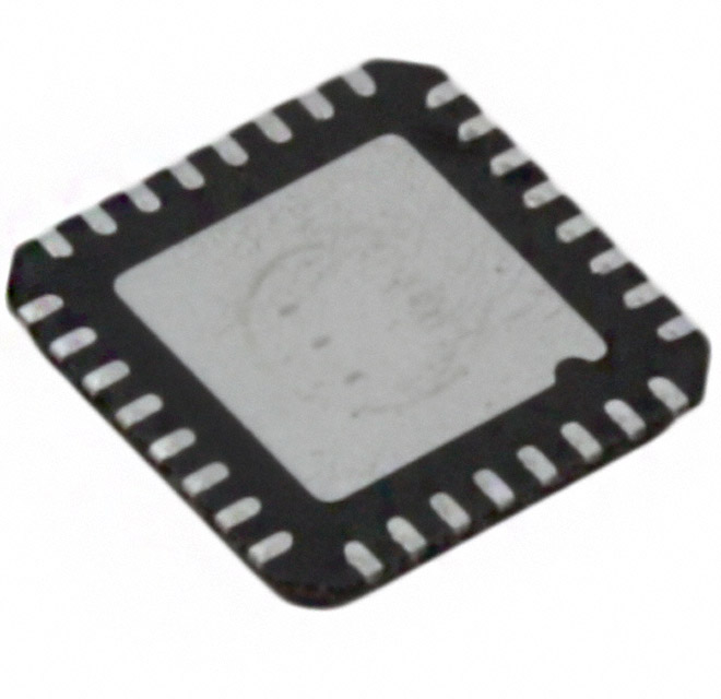
Features: Matched pair of multiplying VGAs Broad frequency range 20 MHz to 2.4 GHz Continuous magnitude control from +5 dB to −30 dB Output third-order intercept 24 dBm Output 1 dB compression point 11 dBm Output noise floor −148 dBm/Hz Adjustable modulation bandwidth up to 230 MHz Fas...
ADL5390: Features: Matched pair of multiplying VGAs Broad frequency range 20 MHz to 2.4 GHz Continuous magnitude control from +5 dB to −30 dB Output third-order intercept 24 dBm Output 1 dB compression...
SeekIC Buyer Protection PLUS - newly updated for 2013!
268 Transactions
All payment methods are secure and covered by SeekIC Buyer Protection PLUS.
Gain Control | Analog |
-3 dB BW (MHz) | 2400MHz |
Gain High End (dB) | +7dB |
Number of Channels | 1 |
Supply Voltage (V) | +5V |
Supply Current | 130mA |
The ADL5390 vector multiplier consists of a matched pair of broadband variable gain amplifiers whose outputs are summed. The separate gain controls for each amplifier are linear-inmagnitude. If the two input RF signals are in quadrature, thevector multiplier can be configured as a vector modulator or as
a variable attenuator/phase shifter by using the gain control pins as Cartesian variables. In this case, the output amplitude can be controlled from a maximum of +5 dB to less than 30 dB, and the phase can be shifted continuously over the entire 360° range. Since the signal paths are linear, the original modulation on the inputs is preserved. If the two signals are independent, then the vector multiplier can function as a 2:1 multiplexer or can provide fading from one channel to another.
The gain control inputs are dc-coupled with a +/−500 mV differential full-scale range centered about a 500 mV commonmode. The maximum modulation bandwidth is 230 MHz, which can be reduced by adding external capacitors to limit the noise bandwidth on the control lines. Both the RF inputs and outputs can be used differentially or single-ended and must be ac-coupled. The impedance of each VGA RF input is 250 Ω to ground, and the differential output impedance is nominally 50 Ω over the operating frequency range. The DSOP pin allows the output stage to be disabled quickly to protect subsequent stages from overdrive. The ADL5390 operates off supply voltages from 4.75 V to 5.25 V while consuming 135 mA. The ADL5390 is fabricated on Analog Devices' proprietary, high performance 25 GHz SOI complementary bipolar ICprocess. ADL5390 is available in a 24-lead, Pb-free CSP package and operates over a −40°C to +85°C temperature range. Evaluation boards are available.