ADL5310

Features: 2 independent channels optimized for photodiode interfacing 6-decade input dynamic range Law conformance 0.3 dB from 3 nA to 3 mA Temperature-stable logarithmic outputs Nominal slope 10 mV/dB (200 mV/dec), externally scalable Intercepts may be independently set by external resistors Use...

product image

ADL5310 Picture
SeekIC No. : 004275414 Detail

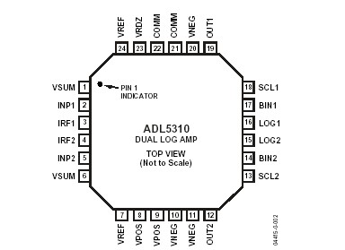
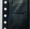
ADL5310: Features: 2 independent channels optimized for photodiode interfacing 6-decade input dynamic range Law conformance 0.3 dB from 3 nA to 3 mA Temperature-stable logarithmic outputs Nominal slope 10 m...
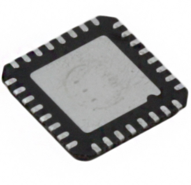
floor Price/Ceiling Price
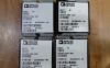
Part Number:
ADL5310
Supply Ability:
5000

Price Break

  • Qty
  • 1~5000
  • Unit Price
  • Negotiable
  • Processing time
  • 15 Days
Total Cost: $ 0.00

SeekIC Buyer Protection PLUS - newly updated for 2013!

  • Escrow Protection.
  • Guaranteed refunds.
  • Secure payments.
  • Learn more >>

Month Sales

268 Transactions

Rating

evaluate  (4.8 stars)

Upload time: 2024/10/17

Payment Methods

All payment methods are secure and covered by SeekIC Buyer Protection PLUS.

Notice: When you place an order, your payment is made to SeekIC and not to your seller. SeekIC only pays the seller after confirming you have received your order. We will also never share your payment details with your seller.
Product Details

Description


Features:

2 independent channels optimized for photodiode interfacing
6-decade input dynamic range Law conformance 0.3 dB from 3 nA to 3 mA
Temperature-stable logarithmic outputs
Nominal slope 10 mV/dB (200 mV/dec), externally scalable
Intercepts may be independently set by external resistors
User-configurable output buffer amplifiers
Single- or dual-supply operation
Space-efficient, 24-lead 4 mm * 4 mm LFCSP
Low power: < 10 mA quiescent current


Application

Gain and absorbance measurements
Multichannel power monitoring
General-purpose baseband log compression


Pinout

  Connection Diagram


Specifications

Parameter Rating
Supply Voltage VP − VN
Input Current
Internal Power Dissipation
JA
Maximum Junction Temperature
Operating Temperature Range
Storage Temperature Range
Lead Temperature Range (Soldering 60 sec)
12 V
20 mA
500 mW
35°C/W1
125°C
40°C to +85°C
−65°C to +150°C
300°C


Description

The ADL53101 low cost, dual logarithmic amplifier converts input current over a wide dynamic range to a linear-in-dB output voltage. It is optimized to determine the optical power in wide-ranging optical communication system applications, including control circuitry for lasers, optical switches, atten-uators, and amplifiers, as well as system monitoring. The device is equivalent to a dual AD8305 with enhanced dynamic range (120 dB). While the ADL5310 contains two independent signal channels with individually configurable transfer function constants (slope and intercept), internal bias circuitry is shared between channels for improved power consumption and channel matching. Dual converters in a single, compact LFCSP package yield space-efficient solutions for measuring gain or attenuation across optical elements. Only a single supply is required; optional dual-supply operation offers added flexibility.

The ADL5310 employs an optimized translinear structure that use the accurate logarithmic relationship between a bipolar transistor's base emitter voltage and collector current, with appropriate scaling by precision currents to compensate for the inherent temperature dependence. Input and reference current pins sink current ranging from 3 nA to 3 mA (limited to ±60 dB between input and reference) into a fixed voltage defined by the VSUM potential. The VSUM potential is internally set to 500 mV but may be externally grounded for dual-supply opera-tion, and for additional applications requiring voltage inputs.

The logarithmic slope of ADL5310 is set to 10 mV/dB (200 mV/decade) nominal and can be modified using external resistors and the independent buffer amplifiers. The logarithmic intercepts for each channel are defined by the individual reference currents, which are set to 3 A nominal for maximum input range by connecting 665 k resistors between the 2.5 V VREF pins and the IRF1 and IRF2 inputs. Tying VRDZ to VREF effectively sets the x-intercept four decades below the reference current-typically 300 pA for a 3 µA reference.

The use of individually optimized reference currents may be valuable when using the ADL5310 for gain or absorbance measurements where each channel input has a different current-range requirement. The reference current inputs are also fully functional dynamic inputs, allowing log ratio operation with the reference input current as the denominator. The ADL5310 is specified for operation from 40°C to +85°C.


Customers Who Bought This Item Also Bought

Margin,quality,low-cost products with low minimum orders. Secure your online payments with SeekIC Buyer Protection.
Isolators
Soldering, Desoldering, Rework Products
Inductors, Coils, Chokes
Static Control, ESD, Clean Room Products
Programmers, Development Systems
Prototyping Products
DE1
View more