Features:
Low Leakage (<100 pA)
Fast Switching Times
Low Charge Injection
TTL/CMOS Compatible
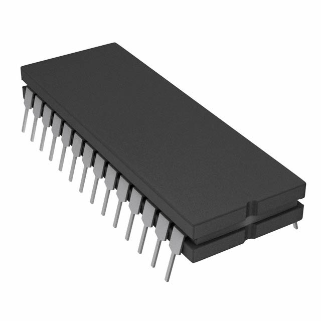
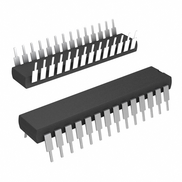
16-Lead DIP or SOIC PackageApplicationBattery Powered Instruments
Single Supply Systems
Remote Powered Equipment
+5 V Supply Systems
Computer Peripherals such as Disk Drives
Precision Instrumentation
Audio and Video Switching
Automatic Test Equipment
Precision Data Acquisition
Sample Hold Systems
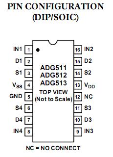
Communication SystemsPinout SpecificationsVDD to VSS . . . . . . . . . . . . . . . . . . . . . . . . . . . . . . . . . . +44 V
VDD to GND . . . . . . . . . . . . . . . . . . . . . . . . . . 0.3 V to +25 V
VSS to GND . . . . . . . . . . . . . . . . . . . . . . . . . . .+0.3 V to 25 V
Analog, Digital Inputs2. . . . . . . . . . . VSS 2 V to VDD + 2 V or
30 mA, Whichever Occurs First
Continuous Current, S or D . . . . . . . . . . . . . . . . . . . . . 30 mA
Peak Current, S or D . . . . . . . . . . . . . . . . . . . . . . . . . .100 mA
(Pulsed at 1 ms, 10% Duty Cycle max)
Operating Temperature Range
Industrial (B Version) . . . . . . . . . . . . . . . . . 40°C to +85°C
Extended (T Version) . . . . . . . . . . . . . . . . 55°C to +125°C
Storage Temperature Range . . . . . . . . . . 65°C to +150°C
Junction Temperature . . . . . . . . . . . . . . . . . . . . . . .. +150°C
Cerdip Package, Power Dissipation . . . . . . . . . . . . . 900 mW
JA Thermal Impedance . . . . . . . . . . . . . . . . . . . . . . 76°C/W
Lead Temperature, Soldering (10 sec) . . . . . . . . . . . +300°CDescriptionThe ADG511, ADG512 and ADG513 are monolithic CMOS ICs containing four independently selectable analog switches. These switches feature low, well-controlled on resistance and wide analog signal range, making them ideal for precision analog signal switching. These switch arrays are fabricated using Analog Devices' advanced linear compatible CMOS (LC
2 MOS) process which offers the additional benefits of low leakage currents, ultralow power dissipation and low capacitance for fast switching speeds with minimum charge injection. These features make the ADG511, ADG512 and ADG513 the optimum choice for a wide variety of signal switching tasks in precision analog signal processing and data acquisition systems.
The ability to operate from single +3 V, +5 V or ±5 V bipolar supplies make the ADG511, ADG512 and ADG513 perfect for use in battery-operated instruments, 420 mA loop systems and with the new generation of DACs and ADCs from Analog Devices. The use of 5 V supplies and reduced operating currents give much lower power dissipation than devices operating from ±15 V supplies.The ADG511, ADG512 and ADG513 contain four independent SPST switches. The ADG511 and ADG512 differ only in that the digital control logic is inverted. The ADG511 switch is turned on with a logic low on the appropriate control input, while a logic high is required for the ADG512. The ADG513 contains two switches whose digital control logic is similar to that of the ADG511 while the logic is inverted in the remaining two switches.

 ADG512 Data Sheet
