Features:
Fast Switching Times
tON 250 ns max
tOFF 250 ns max
Low Power Dissipation (3.3 mW max)
Fault and Overvoltage Protection (40 V to +55 V)
All Switches OFF with Power Supply OFF
Analog Output of ON Channel Clamped Within Power Supplies If an Overvoltage Occurs
Latch-Up Proof Construction
Break Before Make Construction
TTL and CMOS Compatible InputsApplicationExisting Multiplexer Applications (Both Fault-Protected and Nonfault-Protected)
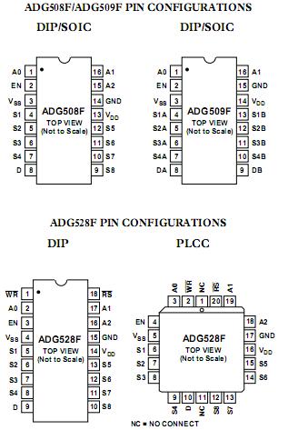
New Designs Requiring Multiplexer FunctionsPinout
 Specifications
| Sw/Mx Function x # |
(8:1) x 1 |
| Interface Type |
Parallel |
| Available Packages |
DIP,SOIC |
| Max Analog Signal Range |
Vss+3V to Vdd-1.5V |
| Ron (Ohms) |
300Ohms |
| Ron Match (Ohms) |
15Ohms |
| Cs (OFF) |
5pF |
| Cs, Cd (ON) |
n/a |
| Off Isolation (-dB) |
68dB |
| Bandwidth |
n/a |
VDD to VSS . . . . . . . . . . . . . . . . . . . . . . . . . . . . . . . . . . .+44 V
VDD to GND . . . . . . . . . . . . . . . . . . . . . . . . . . 0.3 V to +25 V
VSS to GND . . . . . . . . . . . . . . . . . . . . . . . . . . . +0.3 V to 25 V
VEN, VA Digital Input . . . . . . . 0.3 V to VDD + 2 V or 20 mA,
Whichever Occurs First
VS, Analog Input Overvoltage with Power ON . . . . VSS 25 V
to VDD + 40 V
VS, Analog Input Overvoltage with Power OFF
. . . . . . . . . . . . . . . . . . . . . . . . . . . . . . . . . . . . 40 V to +55 V
Continuous Current, S or D . . . . . . . . . . . . . . . . . . . . . 20 mA
Peak Current, S or D
(Pulsed at 1 ms, 10% Duty Cycle max) . . . . . . . . . . . 40 mA
Operating Temperature Range
Industrial (B Version) . . . . . . . . . . . . . . . .. 40°C to +85°C
Extended (T Version) . . . . . . . . . . . . . .. . 55°C to +125°C
Storage Temperature Range . . . . . . . . .. . 65°C to +150°C
Junction Temperature . . . . . . . . . . . . . . . . . . . . . . . +150°C
Cerdip Package
JA, Thermal Impedance
16-Lead . . . . . . . . . . . . . . . . . . . . . . . . . . . .. . . . 76°C/W
18-Lead . . . . . . . . . . . . . . . . . . . . . . . . . . . . . . . . 73°C/W
Lead Temperature, Soldering (10 sec) . . . . . . .. . . +300°C
Plastic Package
JA, Thermal Impedance
16-Lead . . . . . . . . . . . . . . . . . . . . . . . . . . . . . . . . . 117°C
18-Lead . . . . . . . . . . . . . . . . . . . . . . . . . . . . . . . . . 110°C
Lead Temperature, Soldering (10 sec) . . . . . . . . . . +260°CDescriptionThe ADG508F, ADG509F and ADG528F are CMOS analog multiplexers, the ADG508F, ADG509F and ADG528F comprising eight single channels and the product comprising four differential channels. These multiplexers provide fault protection. Using a series n-channel, p-channel, n-channel MOSFET structure, both device and signal source protection is provided in the event of an overvoltage or power loss. The multiplexer can withstand continuous overvoltage inputs from 40 V to +55 V. During fault conditions, the multiplexer input (or output) appears as an open circuit and only a few nanoamperes of leakage current will
flow. This protects not only the multiplexer and the circuitry driven by the multiplexer, but also protects the sensors or signal sources that drive the multiplexer.
The ADG508F, ADG509F and ADG528F switch one of eight inputs to a common output as determined by the 3-bit binary address lines A0, A1 and A2. The ADG509F switches one of four differential inputs to a common differential output as determined by the 2- bit binary address lines A0 and A1. The ADG508F, ADG509F and ADG528F have on-chip
address and control latches that facilitate microprocessor interfacing. An EN input on each device is used to enable or disable the device. When disabled, all channels are switched OFF.

 ADG508F Data Sheet