DescriptionThe ADG506AKP belongs to ADG506A and ADG507A family which are CMOS monolithic analog multiplexers with 16 channels and dual 8 channels, respectively. The ADG506A and ADG507A are designed on an enhanced LC 2 MOS process, which gives an increased signal capability of V SS to V DD and enables operation over a wide range of supply voltages. The devices can operate comfortably anywhere in the 10.8 V to 16.5 V single or dual supply range. These multiplexers also feature high switching speeds and low R ON. The ADG506AKP switches one of 16 inputs to a common output, depending on the state of four binary addresses and an enable input while the ADG507A switches one of eight differential inputs to a common differential output, depending on the state of three binary addresses and an enable input. Both devices have TTL and 5 V CMOS logic compatible digital inputs.
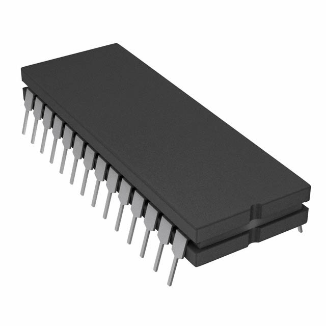
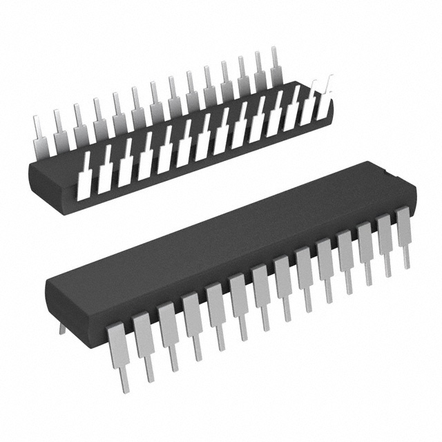
The features of ADG506AKP can be summarized as (1)44 V supply maximum rating; (2)VSS to VDD analog signal range; (3)single/dual supply specifications; (4)wide supply ranges (10.8 V to 16.5 V); (5)extended plastic temperature range (40°C to +85°C); (6)low power dissipation (28 mW max); (7)low leakage (20 pA typ); (8)available in 28-Lead DIP, SOIC, PLCC, TSSOP and LCCC packages; (9)superior alternative to: DG506A, Hl-506 DG507A, Hl-507.
The absolute maximum ratings of ADG506AKP are (1)VDD to V SS: 44 V; (2)VDD to GND: 25 V; (3)VSS to GND: 25 V; (4)analog inputs 2 voltage at S, D : V SS 2 V to V DD + 2 V or 20 mA, whichever occurs first; (5)continuous current, S or D: 20 mA; (6)pulsed current S or D 1 ms duration, 10% duty cycle: 40 mA; (7)digital inputs voltage at A, EN: VSS 4 V to V DD + 4 V or 20 mA, whichever occurs first; (8)power dissipation (any package) up to +75°C : 470 mW, derates above +75°C by: 6 mW/°C; (9)operating temperature commercial (K Version) 40°C to +85°C, industrial (B Version): 40°C to +85°C, extended (T Version) : 55°C to +125°C; (10)storage temperature range: 65°C to +150°C; (11)lead temperature (soldering, 10 secs): +300°C.

 ADG506AKP PLCC28 Data Sheet


