Features: Signal Paths Open Circuit with Power Off
Signal Path Resistance of RON with Power On
44 V Supply Maximum Ratings
Low On Resistance
1 nA Max Path Current Leakage @ +258
Low RON Match (5 V max)
Low Power Dissipation 0.8 mW typ
Latch-Up Proof ConstructionApplicationATE Equipment
Sensitive Measurement Equipment
Hot-Insertion Rack SystemsPinout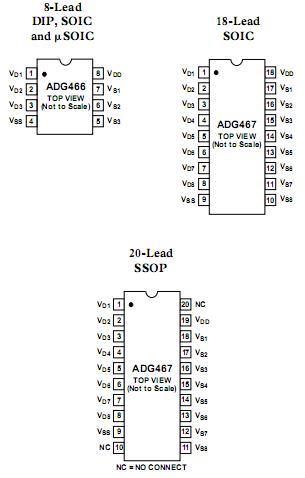 SpecificationsVDD to VSS . . . . . . . . . . . . . . . . . . . . . . . . . . . . . . . . . . +44 V
VS, VD, Analog Input Overvoltage with Power ON2
. . . . . . . . . . . . . . . . . . . . . . . . . . . .VSS 20 V to VDD + 20 V
VS, VD, Analog Input Overvoltage with Power OFF2
. . . . . . . . . . . . . . . . . . . . . . . . . . . . . . . . . . . .35 V to +35 V
Continuous Current, S or D . . . . . . . . . . . . . . . . . . . . .20 mA
Peak Current, S or D . . . . . . . . . . . . . . . . . . . . . . . . . . 40 mA
(Pulsed at 1 ms, 10% Duty Cycle Max)
Operating Temperature Range
Industrial (B Version) . . . . . . . . . . . . . . . . . 40°C to +85°C
Storage Temperature Range . . . . . . . . . . 65°C to +125°C
Junction Temperature . . . . . . . . . . . . . . . . . . . . . . . +150°C
Plastic DIP Package
JA, Thermal Impedance . . . . . . . . . . . . . . . . . . .. 125°C/W
Lead Temperature, Soldering (10 sec) . . . . . . . . . +260°C
SOIC Package
JA, Thermal Impedance . . . . . . . . . . . . . . . . . . . 160°C/W
Lead Temperature, Soldering
Vapor Phase (60 sec) . . . . . . . . . . . . . . . . . . . . . . +215°C
Infrared (15 sec) . . . . . . . . . . . . . . . . . . . . . . . . . +220°C
µSOIC Package
JA, Thermal Impedance . . . . . . . . . . . . . . . . . . 160°C/W
Lead Temperature, Soldering
Vapor Phase (60 sec) . . . . . . . . . . . . . . . . . . . . . .+215°C
Infrared (15 sec) . . . . . . . . . . . . . . . . . . . . . . . . . +220°C
SSOP Package
JA, Thermal Impedance . . . . . . . . . . . . . . . . . . 130°C/W
Lead Temperature, Soldering
Vapor Phase (60 sec) . . . . . . . . . . . . . . . . . . . . . +215°C
Infrared (15 sec) . . . . . . . . . . . . . . . . . . . . . . . . +220°CDescriptionThe ADG466 and ADG467 are triple and octal channel protectors, respectively. The channel protector is placed in series with the signal path. The channel protector will protect sensitive components from voltage transience in the signal path whether the power supplies are present or not. Because the channel
protection works whether the supplies are present or not, the channel protectors are ideal for use in applications where correct power sequencing can't always be guaranteed (e.g., hot-insertion rack systems) to protect analog inputs. ADG466 and ADG467 are discussed further, and some example circuits are given in the
Applications section of this data sheet.
ADG466 and ADG467 have an independent operation and consists of an n-channel MOSFET, a p-channel MOSFET and an n-channel MOSFET, connected in series. The channel protector behaves just like a series resistor during normal operation, i.e., (V
SS + 2 V) < V
IN < (V
DD 1.5 V). When a channel's analog input exceeds the power supplies (including V
DD and V
SS =0 V), one of the MO
SFETs will switch off, clamping the output to either V
SS + 2 V or V
DD 1.5 V. Circuitry and signal source protection is provided in the event of an overvoltage or power loss. The channel protectors can withstand overvoltage inputs
from 40 V to +40 V. See the Circuit Information section of this data sheet.

 ADG467 Data Sheet