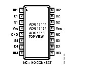
Features: 33 V supply range Fully specified at +12 V, ±15 V 130 on resistance No VL supply required 3 V logic-compatible inputs Rail-to-rail operation 16-lead TSSOP and 16-lead SOIC Typical power consumption: <0.03 WApplicationSignal switchingBattery-powered systemsCommunication systemsAudio/...
ADG1313: Features: 33 V supply range Fully specified at +12 V, ±15 V 130 on resistance No VL supply required 3 V logic-compatible inputs Rail-to-rail operation 16-lead TSSOP and 16-lead SOIC Typical power ...
SeekIC Buyer Protection PLUS - newly updated for 2013!
268 Transactions
All payment methods are secure and covered by SeekIC Buyer Protection PLUS.
Parameter | Rating |
VDD to VSS VDD to GND VSS to GND Analog Inputs1 Digital Inputs1 Peak Current, S or D Continuous Current per Channel, S or D Operating Temperature Range Automotive Storage Temperature Range Junction Temperature 16-Lead TSSOP, JA Thermal Impedance (4-layer board) 16-Lead SOIC, JA Thermal Impedance Reflow Soldering Peak Temperature, Pb free |
35 V |
The ADG1311/ADG1312/ADG1313 are monolithic CMOS devices containing four independently selectable switches designed on a CMOS process.
The ADG1311/ADG1312/ADG1313 contain four independent single-pole/single-throw (SPST) switches. The ADG1311 and ADG1312 differ only in that the digital control logic is inverted. The product switches are turned on with Logic 0 on the appro-priate control input, while Logic 1 is required for the product. The product has two switches with digital control logic similar to the ADG1311; the logic is inverted on the other two switches. The product exhibits break-before-make switching action for use in multiplexer applications.
Each ADG1311/ADG1312/ADG1313 switch conducts equally well in both directions when on and has an input signal range that extends to the supplies. In the off condition, signal levels up to the supplies are blocked.