ADF4001

Features: 200 MHz Bandwidth2.7 V to 5.5 V Power SupplySeparate Charge Pump Supply (VP) Allows Extended Tuning Voltage in 5 V SystemsProgrammable Charge Pump Currents3-Wire Serial InterfaceHardware and Software Power-Down ModeAnalog and Digital Lock DetectHardware-Compatible to the ADF4110/ADF4111/...

product image

ADF4001 Picture
SeekIC No. : 004274617 Detail

ADF4001: Features: 200 MHz Bandwidth2.7 V to 5.5 V Power SupplySeparate Charge Pump Supply (VP) Allows Extended Tuning Voltage in 5 V SystemsProgrammable Charge Pump Currents3-Wire Serial InterfaceHardware a...

floor Price/Ceiling Price

Part Number:
ADF4001
Supply Ability:
5000

Price Break

  • Qty
  • 1~5000
  • Unit Price
  • Negotiable
  • Processing time
  • 15 Days
Total Cost: $ 0.00

SeekIC Buyer Protection PLUS - newly updated for 2013!

  • Escrow Protection.
  • Guaranteed refunds.
  • Secure payments.
  • Learn more >>

Month Sales

268 Transactions

Rating

evaluate  (4.8 stars)

Upload time: 2024/11/6

Payment Methods

All payment methods are secure and covered by SeekIC Buyer Protection PLUS.

Notice: When you place an order, your payment is made to SeekIC and not to your seller. SeekIC only pays the seller after confirming you have received your order. We will also never share your payment details with your seller.
Product Details

Description


Features:

200 MHz Bandwidth
2.7 V to 5.5 V Power Supply
Separate Charge Pump Supply (VP) Allows Extended Tuning Voltage in 5 V Systems
Programmable Charge Pump Currents
3-Wire Serial Interface
Hardware and Software Power-Down Mode
Analog and Digital Lock Detect
Hardware-Compatible to the ADF4110/ADF4111/ADF4112/ADF4113
Typical Operating Current 4.5 mA
Ultralow Phase Noise
16-Lead TSSOP
20-Lead Chip Scale Package


Application

Clock Generation
Low Frequency PLLs
Low Jitter Clock Source
Clock Smoothing
Frequency Translation
SONET, ATM, ADM, DSLAM, SDM


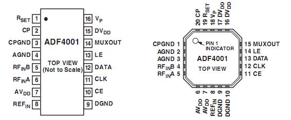
Pinout

  Connection Diagram

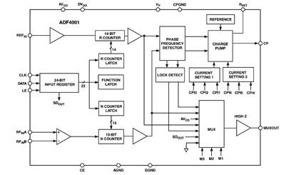
ADF4001 Diagram


Specifications

AVDD to GND3. . . . . . . . . . . . . . . . . . . . . . . . 0.3 V to +7 V
AVDD to DVDD . . . . . . . . . . . . . . . . . . . . . . . . 0 V to + 0.3 V
VP to GND . . . . . . . . . . . . . . . . . . . . . . . . . . . 0.3 V to +7 V
VP to AVDD . . . . . . . . . . . . . . . . . . . . . . . . . 0.3 V to +5.5 V
Digital I/O Voltage to GND . . . . . . . . .0.3 V to VDD + 0.3 V
Analog I/O Voltage to GND . . . . . . . . . .0.3 V to VP + 0.3 V
REFIN, RFINA, RFINB to GND . . . . . . . 0.3 V to VDD + 0.3 V
RFINA to RFINB . . . . . . . . . . . . . . . . . . . . . . . . . . . .±320 mV
Operating Temperature Range
Industrial (B Version) . . . . . . . . . . . . . . . . 40°C to +85°C
Storage Temperature Range . . . . . . . . . . .65°C to +150°C
Maximum Junction Temperature . . . . . . . . . . . . . . . . . 150°C


Type Single Integer-N
Max RF Input (MHz) 200MHz
Norm Phase Noise (dBc/Hz) -214dBc
Max REFin (MHz) 104MHz
RF Prescalers n/a
Supply Current 4.5mA
Package 16-Lead TSSOP,20-Lead CSP


Description

The ADF4001 clock generator can be used to implement clock sources for PLLs that require very low noise, stable reference signals. ADF4001 consists of a low-noise digital PFD (Phase Frequency Detector), a precision charge pump, a programmable reference divider, and a programmable 13-bit N counter. In addition, the 14-bit reference counter (R Counter) allows selectable REFIN frequencies at the PFD input. A complete PLL (Phase-Locked Loop) can be implemented if the synthesizer is used with an external loop filter and VCO (Voltage Controlled Oscillator) or VCXO (Voltage Controlled Crystal Oscillator). The N min value of 1 allows flexibility in clock generation.


Customers Who Bought This Item Also Bought

Margin,quality,low-cost products with low minimum orders. Secure your online payments with SeekIC Buyer Protection.
Hardware, Fasteners, Accessories
Cables, Wires - Management
Inductors, Coils, Chokes
Power Supplies - External/Internal (Off-Board)
Transformers
Prototyping Products
DE1
View more