ADC14V155

Features: 1.1 GHz Full Power Bandwidth Internal sample-and-hold circuit Low power consumption Internal precision 1.0V reference Single-ended or Differential clock modes Clock Duty Cycle Stabilizer Dual +3.3V and +1.8V supply operation Power-down and Sleep modes Offset binary or 2's complement out...

product image

ADC14V155 Picture
SeekIC No. : 004274191 Detail

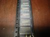
ADC14V155: Features: 1.1 GHz Full Power Bandwidth Internal sample-and-hold circuit Low power consumption Internal precision 1.0V reference Single-ended or Differential clock modes Clock Duty Cycle Stabilizer ...

floor Price/Ceiling Price

Part Number:
ADC14V155
Supply Ability:
5000

Price Break

  • Qty
  • 1~5000
  • Unit Price
  • Negotiable
  • Processing time
  • 15 Days
Total Cost: $ 0.00

SeekIC Buyer Protection PLUS - newly updated for 2013!

  • Escrow Protection.
  • Guaranteed refunds.
  • Secure payments.
  • Learn more >>

Month Sales

268 Transactions

Rating

evaluate  (4.8 stars)

Upload time: 2024/6/2

Payment Methods

All payment methods are secure and covered by SeekIC Buyer Protection PLUS.

Notice: When you place an order, your payment is made to SeekIC and not to your seller. SeekIC only pays the seller after confirming you have received your order. We will also never share your payment details with your seller.
Product Details

Description


Features:

1.1 GHz Full Power Bandwidth
Internal sample-and-hold circuit
Low power consumption
Internal precision 1.0V reference
Single-ended or Differential clock modes
Clock Duty Cycle Stabilizer
Dual +3.3V and +1.8V supply operation
Power-down and Sleep modes
Offset binary or 2's complement output data format
Dual Data Rate (DDR) LVDS outputs
Pin-compatible: ADC12V170
48-pin LLP package, (7x7x0.8mm, 0.5mm pin-pitch)


Application

High IF Sampling Receivers
Wireless Base Station Receivers
Power Amplifier Linearization
Multi-carrier, Multi-mode Receivers
Test and Measurement Equipment
Communications Instrumentation
Radar Systems


Pinout

  Connection Diagram


Specifications

Resolution 14 bits
Channels 1 Channels
SNR 71.7 dB
SFDR 86.9 dB
ENOB 11.5 bits
Max Sample Rate 155 MSPS
Min Sample Rate 5 MSPS
Power Dissipation 0.951 Watt
PowerWise Rating 1 2.12 pJ/conv
INL (+/-) 2.4 LSB
SINAD 71.2 dB
DNL (+/-) 0.55 LSB
THD dB -82.2 dB
Min Supply Voltage 3 Volt
Max Supply Voltage 3.6 Volt
Nominal Vin 2 Vpp
Temperature Min -40 deg C
Temperature Max 85 deg C
Data Converter Type ADC
PowerWise Yes
View Using Catalog


If Military/Aerospace specified devices are required, please contact the National Semiconductor Sales Office/ Distributors for availability and specifications.
Supply Voltage (VA, VD)............ −0.3V to 4.2V
Supply Voltage (VDR) .............−0.3V to 2.35V
|VAVD| ......................... 100 mV
Voltage on Any Input Pin
(Not to exceed 4.2V)...........−0.3V to (VA +0.3V)
Voltage on Any Output Pin
(Not to exceed 2.35V)..........-0.3V to (VDR +0.2V)
Input Current at Any Pin other
than Supply Pins (Note 3)..................5 mA
Package Input Current (Note 3) ............±50 mA
Max Junction Temp (TJ) ..................+150
Thermal Resistance (JA) ................24°/W
Package Dissipation at TA = 25 (Note 4)........5.2W
ESD Rating
Human Body Model (Note 5) ................2000 V
Machine Model (Note 5)....................200 V
Charge Device Model .................... 1000 V
Storage Temperature ..............−65°C to +150

Soldering process must comply with National Semiconductor's Reflow Temperature Profile specifications. Refer to www.national.com/packaging.


Description

The ADC14V155 is a high-performance CMOS analog-todigital converter with LVDS outputs. It is capable of converting analog input signals into 14-Bit digital words at rates up to 155 Mega Samples Per Second (MSPS). Data leaves the chip in a DDR (Dual Data rate) format; this allows both edges of the output clock to be utilized while achieving a smaller package size. This converter uses a differential, pipelined architecture with digital error correction and an on-chip sample-and-hold circuit to minimize power consumption and the external component count, while providing excellent dynamic performance. A unique sample-and-hold stage yields a full-power bandwidth of 1.1 GHz. The ADC14V155 operates from dual +3.3V and +1.8V power supplies and consumes 951 mW of power at 155 MSPS.

The separate +1.8V supply for the digital output interface allows lower power operation with reduced noise. A powerdown feature reduces the power consumption to 15 mW while still allowing fast wake-up time to full operation. In addition there is a sleep feature which consumes 50 mW of power and has a faster wake-up time.

The differential inputs provide a full scale differential input swing equal to 2 times the reference voltage. A stable 1.0V internal voltage reference is provided, or the ADC14V155 can be operated with an external reference.

Clock mode (differential versus single-ended) and output data format (offset binary versus 2's complement) are pin-selectable. A duty cycle stabilizer maintains performance over a wide range of input clock duty cycles.

The ADC14V155 is pin-compatible with the ADC12V170. It is available in a 48-lead LLP package and operates over the industrial temperature range of −40 to +85.


Customers Who Bought This Item Also Bought

Margin,quality,low-cost products with low minimum orders. Secure your online payments with SeekIC Buyer Protection.
Industrial Controls, Meters
Prototyping Products
DE1
Soldering, Desoldering, Rework Products
Power Supplies - External/Internal (Off-Board)
Discrete Semiconductor Products
Memory Cards, Modules
View more