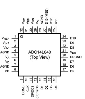
Features: · Single +3.3V supply operation·Internal sample-and-hold· Internal reference·Outputs 2.4V to 3.6V compatible· Duty Cycle StabilizeApplication· Medical Imaging· Instrumentation· Communications· Digital VideoPinoutSpecificationsIf Military/Aerospace specified devices are required, please c...
ADC14L040: Features: · Single +3.3V supply operation·Internal sample-and-hold· Internal reference·Outputs 2.4V to 3.6V compatible· Duty Cycle StabilizeApplication· Medical Imaging· Instrumentation· Communicati...
SeekIC Buyer Protection PLUS - newly updated for 2013!
268 Transactions
All payment methods are secure and covered by SeekIC Buyer Protection PLUS.
If Military/Aerospace specified devices are required, please contact the National Semiconductor Sales Office/ Distributors for availability and specifications.
VA, VD, VDR................................. 4.2V
|VAVD| .......................... 100 mV
Voltage on Any Input or Output.......−0.3V to (VA or VD+0.3V)
Input Current at Any Pin (Note 3).............. ±25 mA
Package Input Current (Note 3) ...............±50 mA
Package Dissipation at TA = 25°C ............See (Note 4)
ESD Susceptibility
Human Body Model (Note 5)...................2500V
Machine Model (Note 5)......................250V
Storage Temperature ...............−65°C to +150°C
Soldering process must comply with National Semiconductor's Reflow Temperature Profile specifications. Refer to www.national.com/packaging.
Resolution | 14 bits |
Channels | 1 Channels |
SNR | 74 dB |
SFDR | 90 dB |
ENOB | 12 bits |
Max Sample Rate | 40 MSPS |
Min Sample Rate | 5 MSPS |
Power Dissipation | 0.235 Watt |
PowerWise Rating 1 | 1.43 pJ/conv |
INL (+/-) | 1.5 LSB |
SINAD | 73.5 dB |
DNL (+/-) | 0.5 LSB |
THD dB | -86 dB |
Min Supply Voltage | 3 Volt |
Max Supply Voltage | 3.6 Volt |
Nominal Vin | 2 Vpp |
Temperature Min | -40 deg C |
Temperature Max | 85 deg C |
Data Converter Type | ADC |
PowerWise | Yes |
View Using Catalog |
The ADC14L040 is a low power monolithic CMOS analogto- digital converter capable of converting analog input signals into 14-bit digital words at 40 Megasamples per second (MSPS). These converters use a differential, pipeline architecture with digital error correction and an on-chip sampleand- hold circuit to minimize power consumption while providing excellent dynamic performance and a 150 MHz Full Power Bandwidth. Operating on a single +3.3V power supply, the ADC14L040 achieves 11.9 effective bits at nyquist and consumes just 235 mW at 40 MSPS . The Power Down feature reduces power consumption to 15 mW.
The differential inputs of ADC14L040 provide a full scale differential input swing equal to 2 times VREF with the possibility of a singleended input. Full use of the differential input is recommended for optimum performance. Duty cycle stabilization and output data format are selectable using a quad state function pin. The output data can be set for offset binary or two's complement.
To ease interfacing to lower voltage systems, the digital output driver power pins of the ADC14L040 can be connected to a separate supply voltage in the range of 2.4V to the analog supply voltage.
This device ADC14L040 is available in the 32-lead LQFP package and will operate over the industrial temperature range of −40°C to +85°C. An evaluation board is available to ease the evaluation process.