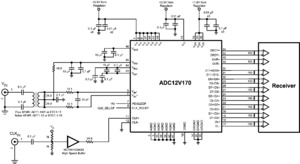
Pinout Specifications
| Resolution | 12 bits |
| Channels | 1 Channels |
| SNR | 67.2 dB |
| SFDR | 85.8 dB |
| ENOB | 10.9 bits |
| Max Sample Rate | 170 MSPS |
| Min Sample Rate | 5 MSPS |
| Power Dissipation | 0.781 Watt |
| PowerWise Rating 1 | 2.40 pJ/conv |
| INL (+/-) | 0.5 LSB |
| SINAD | 67.1 dB |
| DNL (+/-) | 0.3 LSB |
| THD dB | -82.3 dB |
| Min Supply Voltage | 3 Volt |
| Max Supply Voltage | 3.6 Volt |
| Nominal Vin | 2 Vpp |
| Temperature Min | -40 deg C |
| Temperature Max | 85 deg C |
| Data Converter Type | ADC |
| PowerWise | Yes |
| View Using Catalog |
DescriptionThe ADC12V170 is a high-performance CMOS analog-to-digital converter with LVDS outputs. It is capable of converting analog input signals into 12-Bit digital words at rates up to 170 Mega Samples Per Second (MSPS). Data leaves the chip in a DDR (Dual Data Rate) format; this allows both edges of the output clock to be utilized while achieving a smaller package size. This converter uses a differential, pipelined architecture with digital error correction and an on-chip sample-and-hold circuit to minimize power consumption and the external component count, while providing excellent dynamic performance. A unique sample-and-hold stage yields a full-power bandwidth of 1.1 GHz. The ADC12V170 operates from dual +3.3V and +1.8V power supplies and consumes 781 mW of power at 170 MSPS.
The separate +1.8V supply for the digital output interface allows lower power operation with reduced noise. A power-down feature reduces the power consumption to 15 mW while still allowing fast wake-up time to full operation. In addition there is a sleep feature which consumes 50 mW of power and has a faster wake-up time.
The differential inputs provide a full scale differential input swing equal to 2 times the reference voltage. A stable 1.0V internal voltage reference is provided, or the ADC12V170 can be operated with an external reference.
Clock mode (differential versus single-ended) and output data format (offset binary versus 2's complement) are pin-selectable. A duty cycle stabilizer maintains performance over a wide range of input clock duty cycles.
The ADC12V170 is pin-compatible with the ADC14V155. It is available in a 48-lead LLP package and operates over the industrial temperature range of −40°C to +85°C.
Design Tools
| Title |
Size in Kbytes |
Date |
|
|
|
| Evaluation Systems |
32 Kbytes |
2-Jun-2008 |
View |
|
|
If you have trouble printing or viewing PDF file(s), see Printing Problems.
|

 ADC12V170 Data Sheet


