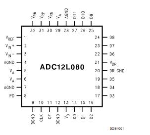
Features: . Single supply operation. Low power consumption. Power down mode. Internal or external reference. Select able Offset Binary or 2's Complement data format. Pin-compatible with ADC12010, ADC12020, ADC12040, ADC12L063, ADC12L066Application. Ultra sound and Imaging. Instrumentation. Cellula...
ADC12L080: Features: . Single supply operation. Low power consumption. Power down mode. Internal or external reference. Select able Offset Binary or 2's Complement data format. Pin-compatible with ADC12010, AD...
SeekIC Buyer Protection PLUS - newly updated for 2013!
268 Transactions
All payment methods are secure and covered by SeekIC Buyer Protection PLUS.
If Military/Aerospace specified devices are required, please contact the National Semiconductor Sales Office/Distributors for availability and specifications.
VA,VD,VDR...............................................................................4.2V
|VAVD|........................................................................... 100mV
VDRVD........................................................................... 300mV
Voltage on AnyPin................................. −0.3V to VA or (VD+0.3V)
Input Current at AnyPin (Note3) .......................................±25mA
Package Input Current (Note3) .........................................±50mA
Package Dissipation at TA=25˚C See (Note4)
ESD Susceptibility
Human Body Model (Note5) ................................................2500V
Machine Model (Note5) .........................................................250V
Soldering Temperature,
Infrared, 10sec. (Note6)...................................................... 235˚C
Storage Temperature .........................................−65˚C to +150˚C
The ADC12L080 is a monolithic CMOS analog-to-digital con-verter capable of converting analog input signals into 12-bit digital words at 80 Megasamplesper second(MSPS). This converter uses a differential, pipe line architecture with digital error correction and anon-chip sample-and-hold circuit to minimize die size and power consumption while providing excellent dynamic performance. The ADC12L080 can be operated with either the internal or an external reference. Operating on a single 3.3V power supply, this device con-sumes just 425mW at 80MSPS, including the reference current.The Power Down feature reduces power consump-tion to just 50mW.
The differential inputs of ADC12L080 provide a full scale input swing equal to ± VREF.The buffered, high impedance,single-ended ex-ternal reference input is converted on-chip to a differential reference for use by the processing circuitry. Output data format maybe select edaseither offset binary or two'scomplement.
This device ADC12L080 is available in the 32-lead LQFP package and operates over the industrial temperature range of −40˚C to +85˚C.