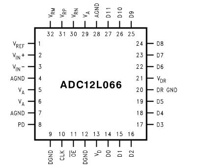
Features: Single supply operationLow power consumptionPower down modeOn-chip reference bufferApplicationUltrasound and ImagingInstrumentationCellular Base Stations/Communications ReceiversSonar/RadarxDSLWireless Local LoopsData Acquisition SystemsDSP Front EndsPinoutSpecificationsVA,VD ,VDR..........
ADC12L066: Features: Single supply operationLow power consumptionPower down modeOn-chip reference bufferApplicationUltrasound and ImagingInstrumentationCellular Base Stations/Communications ReceiversSonar/Rada...
SeekIC Buyer Protection PLUS - newly updated for 2013!
268 Transactions
All payment methods are secure and covered by SeekIC Buyer Protection PLUS.
TheADC12L066isamonolithicCMOSanalog-to-digitalcon- verter capable of converting analog input signals into 12-bit digital words at 66 Megasamples per second (MSPS), mini- mum, with typical operation possible up to 80 MSPS. This converter uses a differential, pipeline architecture with digital error correction and an on-chip sample-and-hold circuit to minimize die size and power consumption while providing excellent dynamic performance. A unique sample-and-hold stage yields a full-power bandwidth of 450 MHz. Operating on a single 3.3V power supply, this device consumes just 357 mW at 66 MSPS, including the reference current. The Power Down feature reduces power consumption to just 50 mW.
The differential inputs of ADC12L066 provide a full scale input swing equal to ±VREF with the possibility of a single-ended input. Full use of the differential input is recommended for optimum perfor-mance. For ease of use, the buffered, high impedance, single-ended reference input is converted on-chip to a differ- ential reference for use by the processing circuitry. Output data format is 12-bit offset binary.
This device ADC12L066 is available in the 32-lead LQFP package and willoperateovertheindustrialtemperaturerangeof-40 to +85. An evaluation board is available to facilitate the evaluation process.