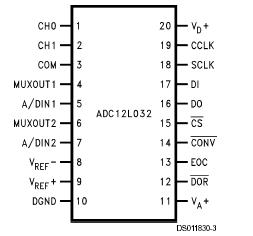
Features: ·0V to 3.3V analog input range with single 3.3V power supply
·Serial I/O ( MICROWIRE and SPI Compatible)
·2, 4, or 8 channel differential or single-ended multiplexer
·Analog input sample/hold function
·Power down mode
·Variable resolution and conversion rate
·Programmable acquisition time
·Variable digital output word length and format
·No zero or full scale adjustment required
·Fully tested and guaranteed with a 2.5V reference
·No Missing Codes over temperatureApplication·Portable Medical instruments
·Portable computing
·Portable Test equipmentPinout
SpecificationsPositive Supply Voltage
(V+ = VA+ = VD+) 6.5V
Voltage at Inputs and Outputs
except CH0CH7 and COM -0.3V to V+ +0.3V
Voltage at Analog Inputs
CH0CH7 and COM GND -5V to V+ +5V
|VA+ - VD+| 300 mV
Input Current at Any Pin (Note 3) ±30 mA
Package Input Current (Note 3) ±120 mA
Package Dissipation at
TA = 25 (Note 4) 500 mW
ESD Susceptability (Note 5)
Human Body Model 1500V
Soldering Information
N Packages (10 seconds) 260
SO Package (Note 6):
Vapor Phase (60 seconds) 215
Infrared (15 seconds) 220
Storage Temperature -65 to +150DescriptionThe ADC12L030 family is 12-bit plus sign successive approximation A/D converters with serial I/O and configurable input multiplexers. These devices are fully tested with a single 3.3V power supply. The ADC12L032, ADC12L034 and ADC12L038 have 2, 4 and 8 channel multiplexers, respectively.
Differential multiplexer outputs and A/D inputs are available on the MUXOUT1, MUXOUT2, A/DIN1 and A/DIN2 pins. The ADC12L030 has a two channel multiplexer with the multiplexer outputs and A/D inputs internally connected. On request, these A/Ds go through a self calibration process that adjusts linearity, zero and full-scale errors to less than ±1/2 LSB each.
The analog inputs of ADC12L032 can be configured to operate in various combinations of single-ended, differential, or pseudo-differential modes. A fully differential unipolar analog input range (0V to +3.3V) can be accommodated with a single +3.3V supply. In the differential modes, valid outputs are obtained even when the negative inputs are greater than the positive because of the 12-bit plus sign two's complimentoutput data format.
The serial I/O is configured to comply with NSC's MICROWIRE™ and Motorola's SPI standards. For voltage references, see the LM4040 or LM4041 data sheets.

 ADC12L032 Data Sheet


