ADC12DS080

PinoutSpecificationsResolution12 bitsChannels2 ChannelsSNR71.2 dBSFDR90 dBENOB11.5 bitsMax Sample Rate80 MSPSMin Sample Rate20 MSPSPower Dissipation0.845 WattPowerWise Rating 11.82 pJ/convINL (+/-)0.5 LSBSINAD71.1 dBDNL (+/-)0.25 LSBTHD dB-88 dBMin Supply Voltage2.7 VoltMax Supply Voltage3.6 VoltN...

product image

ADC12DS080 Picture
SeekIC No. : 004274154 Detail

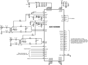
ADC12DS080: PinoutSpecificationsResolution12 bitsChannels2 ChannelsSNR71.2 dBSFDR90 dBENOB11.5 bitsMax Sample Rate80 MSPSMin Sample Rate20 MSPSPower Dissipation0.845 WattPowerWise Rating 11.82 pJ/convINL (+/-)0...

floor Price/Ceiling Price

Part Number:
ADC12DS080
Supply Ability:
5000

Price Break

  • Qty
  • 1~5000
  • Unit Price
  • Negotiable
  • Processing time
  • 15 Days
Total Cost: $ 0.00

SeekIC Buyer Protection PLUS - newly updated for 2013!

  • Escrow Protection.
  • Guaranteed refunds.
  • Secure payments.
  • Learn more >>

Month Sales

268 Transactions

Rating

evaluate  (4.8 stars)

Upload time: 2024/9/16

Payment Methods

All payment methods are secure and covered by SeekIC Buyer Protection PLUS.

Notice: When you place an order, your payment is made to SeekIC and not to your seller. SeekIC only pays the seller after confirming you have received your order. We will also never share your payment details with your seller.
Product Details

Description


Pinout


Specifications

Resolution12 bits
Channels2 Channels
SNR71.2 dB
SFDR90 dB
ENOB11.5 bits
Max Sample Rate80 MSPS
Min Sample Rate20 MSPS
Power Dissipation0.845 Watt
PowerWise Rating 11.82 pJ/conv
INL (+/-)0.5 LSB
SINAD71.1 dB
DNL (+/-)0.25 LSB
THD dB-88 dB
Min Supply Voltage2.7 Volt
Max Supply Voltage3.6 Volt
Nominal Vin2 Vpp
Temperature Min-40 deg C
Temperature Max85 deg C
Data Converter TypeADC
PowerWiseYes
View Using Catalog


Description

The ADC12DS080 is a high-performance CMOS analog-to-digital converter capable of converting two analog input signals into 12-bit digital words at rates up to 80 Mega Samples Per Second (MSPS). The digital outputs are serialized and provided on differential LVDS signal pairs. This converter uses a differential, pipelined architecture with digital error correction and an on-chip sample-and-hold circuit to minimize power consumption and the external component count, while providing excellent dynamic performance. The ADC12DS080 may be operated from a single +3.0V or 3.3V power supply. A power-down feature reduces the power consumption to very low levels while still allowing fast wake-up time to full operation. The differential inputs accept a 2V full scale differential input swing. A stable 1.2V internal voltage reference is provided, or the ADC12DS080 can be operated with an external 1.2V reference. The selectable duty cycle stabilizer maintains performance over a wide range of clock duty cycles. A serial interface allows access to the internal registers for full control of the ADC12DS080's functionality. The ADC12DS080 is available in a 60-lead LLP package and operates over the industrial temperature range of −40°C to +85°C

Design Tools


Title Size in Kbytes Date    
Evaluation Systems 32 Kbytes 2-Jun-2008 View    

If you have trouble printing or viewing PDF file(s), see Printing Problems.


Customers Who Bought This Item Also Bought

Margin,quality,low-cost products with low minimum orders. Secure your online payments with SeekIC Buyer Protection.
Optoelectronics
Discrete Semiconductor Products
Crystals and Oscillators
Programmers, Development Systems
Static Control, ESD, Clean Room Products
View more